

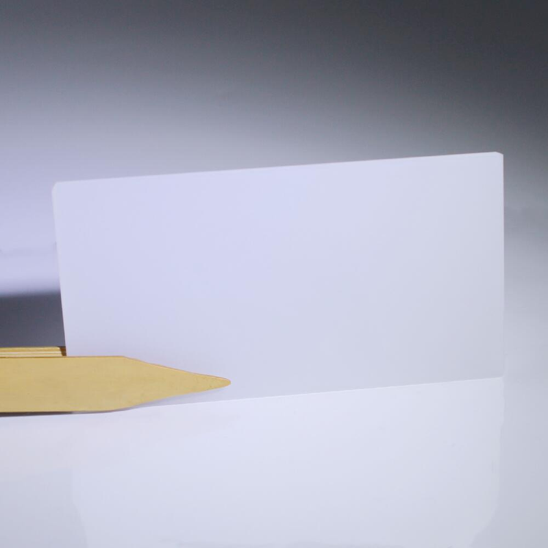
China Single-Crystal Products Optical LiNbO3 Crystal Wafers X-P22L1T14701
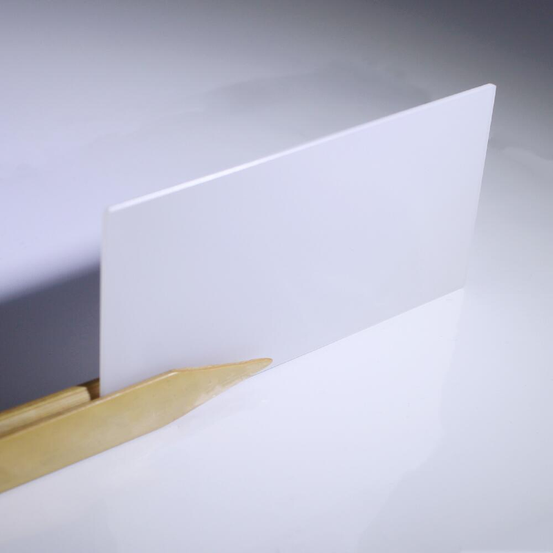
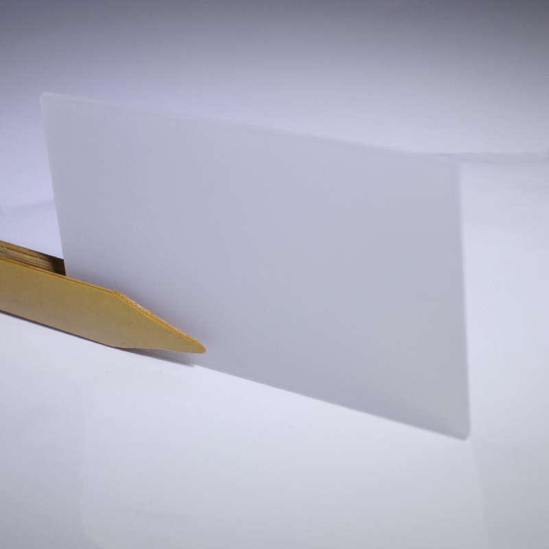
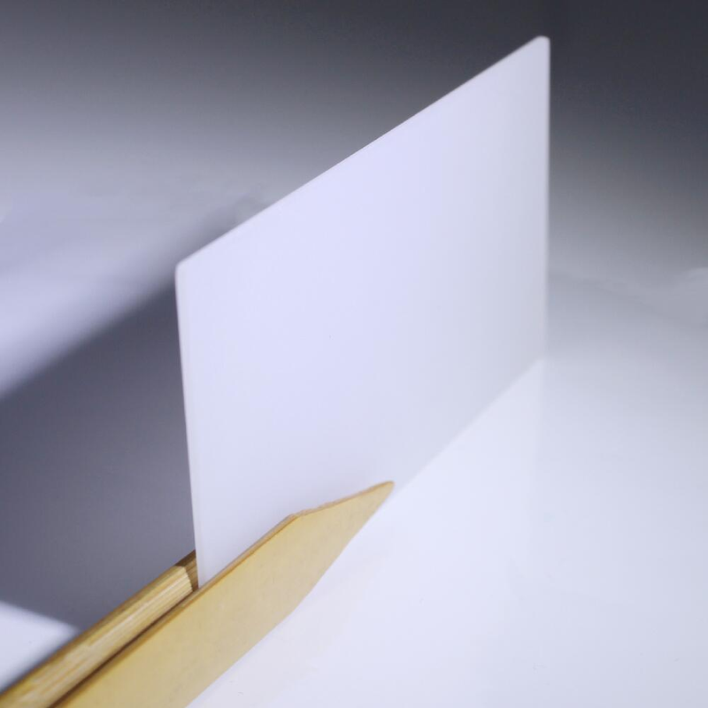
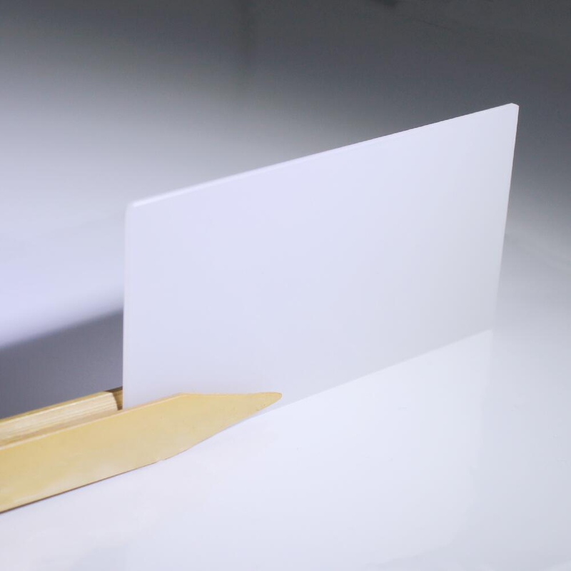
Lithium Niobate (LiNbO3) is a well-developed crystalline material characterized by a high electromechanical coupling coefficient, a wide range of transparency, and excellent chemical and mechanical stability.Single side polishing/double side polishing are all available, cutting angle X/Y/Z etc.They can be used in a wide range of applications including telecommunications and sensing, surface acoustic devices, integrated optics, and novel wavelength generating and refracting elements.VY Optoelectronics Co.,Ltd. can customize various grades and sizes of LiNbO3 wafers according to your requirements. Material: LT, LN etc.. Dimension: 76.20mm Thickness: 0.50mm Surface Accuracy: lambda/8 Surface Quality: 20/10 Tolerance: +/-0.01mm Parallelism: 30″ Lithium niobium crystal (LN)LiNbO3 lens is widely used in SAW filter, optical waveguide, photoelectricity modulator, frequency multiplication transducer and information storage as a functional crystal with excellent physical feature of anti high temperature and anti canker. It has stable mechanical performance, and will appear different special feature after being doped differently. Customization acceptable
 Save to Favorites
Overview
Specifications
| Parameter | Value |
|---|---|
| Cutting Angle [Saw Grade LiNbO3(LN)] | X/Y/Z/Y36/Y42/Y48/X112 etc |
| Diameter/size [Saw Grade LiNbO3(LN);Diameter/size 3”/76.2 mm] | 3”/76.2 |
| Diameter/size [Saw Grade LiNbO3(LN);Diameter/size 4”/100 mm] | 4”/100 |
| Tol(±) [Saw Grade LiNbO3(LN);Diameter/size 3”/76.2 mm] | 0.25 mm |
| Tol(±) [Saw Grade LiNbO3(LN);Diameter/size 4”/100 mm] | 0.5 mm |
| Thickness [Saw Grade LiNbO3(LN);Diameter/size 3”/76.2 mm] | 0.10mm or more |
| Thickness [Saw Grade LiNbO3(LN);Diameter/size 4”/100 mm] | 0.18mm or more |
| Primary reference flat [Saw Grade LiNbO3(LN);Diameter/size 3”/76.2 mm] | 22mm or customized |
| Primary reference flat [Saw Grade LiNbO3(LN);Diameter/size 4”/100 mm] | 32.5mm or customized |
| LTV [Saw Grade LiNbO3(LN);Diameter/size 3”/76.2 mm;5mmx5mm] | < 2 µm |
| LTV [Saw Grade LiNbO3(LN);Diameter/size 4”/100 mm;5mmx5mm] | < 2 µm |
| TTV [Saw Grade LiNbO3(LN);Diameter/size 3”/76.2 mm] | < 8 µm |
| TTV [Saw Grade LiNbO3(LN);Diameter/size 4”/100 mm] | < 10 µm |
| Bow [Saw Grade LiNbO3(LN);Diameter/size 3”/76.2 mm] | ±20 µm |
| Bow [Saw Grade LiNbO3(LN);Diameter/size 4”/100 mm] | ±25 µm |
| Warp [Saw Grade LiNbO3(LN);Diameter/size 3”/76.2 mm] | ≤ 30 % |
| Warp [Saw Grade LiNbO3(LN);Diameter/size 4”/100 mm] | ≤ 40 % |
| PLTV [Saw Grade LiNbO3(LN);Diameter/size 3”/76.2 mm;5mm*5mm] | ≥95%(5mm*5mm) |
| PLTV [Saw Grade LiNbO3(LN);Diameter/size 4”/100 mm;5mm*5mm] | ≥95%(5mm*5mm) |
| Orientation Flat [Saw Grade LiNbO3(LN)] | All available |
| Surface Type [Saw Grade LiNbO3(LN)] | Single Side Polished /Double Sides Polished |
| Polished side Ra [Saw Grade LiNbO3(LN)] | ≤1 nm |
| Back Side Criteria [Saw Grade LiNbO3(LN)] | General is 0.2-0.5 or as customized |
| Edge Rounding [Saw Grade LiNbO3(LN)] | Compliant with SEMI M1.2 Standard/refer to IEC62276 |
| Crystal symmetry [Saw Grade LiNbO3(LN);Basic materials characteristics] | Trigonal, 3m |
| Lattice constant, A [Saw Grade LiNbO3(LN);Basic materials characteristics] | a = 5.154 c = 13.783 |
| Density, g/cm3 [Saw Grade LiNbO3(LN);Basic materials characteristics] | 7.45 g/cm3 |
| Melting point , °C [Saw Grade LiNbO3(LN);Basic materials characteristics] | 1650 °C |
| Curie point , °C [Saw Grade LiNbO3(LN);Basic materials characteristics] | 605 °C |
| Mohs hardness [Saw Grade LiNbO3(LN);Basic materials characteristics] | 6 |
| Thermal expansion coefficient, 10-6/ °C [Saw Grade LiNbO3(LN);Basic materials characteristics] | aa = 16 ac = 4 |
| Thermal conductivity , mW/cm °C [Saw Grade LiNbO3(LN);Basic materials characteristics] | 46 mW/cm °C |
| Dielectric Constant (@ 100 KHz) [Saw Grade LiNbO3(LN);Basic materials characteristics;@100 KHz;@ 100 KHz;@ 100 KHz)] | ea = 54 ec = 43 |
| Refractive indices @ 633 nm [Saw Grade LiNbO3(LN);Basic materials characteristics;@633 nm;@ 633 nm] | no = 2.175 ne = 2.180 |
| Pyroelectric Coefficient [Saw Grade LiNbO3(LN);Basic materials characteristics] | -2.3 10-4 C/°C/m2 |
| Orientation [Optical Grade LN Wafer] | X&Z-cut ±0.2° |
| Diameter [Optical Grade LN Wafer] | 50.8mm/76.2 mm/100mm ±0.3 mm |
| Orientation Flat(OF) [Optical Grade LN Wafer;Perpendicular to X ±0.2°] | 22mm ±2 mm/32mm ±2 mm Perpendicular to X ±0.2° |
| Second Refer.Flat(RF) [Optical Grade LN Wafer] | Cw225°±0.5°from OF Cw315°±0.5°from OF |
| Thickness [Optical Grade LN Wafer] | 250um/500um/1000um ±5um or more |
| Surface Quality [Optical Grade LN Wafer] | Double sides polished; S/D:20/10 |
| TTV [Optical Grade LN Wafer] | ≤10um |
| WARP [Optical Grade LN Wafer] | ≤50um |
| Curie Temperature [Optical Grade LN Wafer] | 1142℃± 0.7℃ |
| Refractive Index [Optical Grade LN Wafer;prism coupler method@632.8nm] | n。=2.2878±0.0002 n。=2.2033±0.0002 prism coupler method@632.8nm |
| Edge Beveling [Optical Grade LN Wafer] | Edge Rounding |
| Crystal Structure [Optical Grade LN Wafer;Basic materials characteristics] | Trigonal, point group 3m |
| Lattice Parameters [Optical Grade LN Wafer;Basic materials characteristics] | a=5.148Å, c=13.863Å |
| Density [Optical Grade LN Wafer;Basic materials characteristics] | 4.64 g/cm3 |
| Melting Point [Optical Grade LN Wafer;Basic materials characteristics] | 1250 °C |
| Curie Point [Optical Grade LN Wafer;Basic materials characteristics] | 1142±2℃ |
| Mohs Hardness [Optical Grade LN Wafer;Basic materials characteristics] | 5 |
| Dielectric Constant [Optical Grade LN Wafer;Basic materials characteristics] | e11/e0 = 85; e33/e0 = 29.5 |
| Thermal Conductitiy [Optical Grade LN Wafer;Basic materials characteristics;at 25°C] | 38 W/m/°C at 25°C |
| Thermal Expansion Coefficient [Optical Grade LN Wafer;Basic materials characteristics;at 25°C] | a1=a2 =2×10⁻⁶/°C, a3=2.2×10⁻⁶/ °C at 25°C |
| Elastic Stiffness Constant [Optical Grade LN Wafer;Basic materials characteristics] | CE11 = 2.04 x 10¹¹ N/m2, CE33 = 2.46 x 10¹¹ N/m2 |
Applications
Datasheet
Please provide your email to download the datasheet.
Invalid email format. Please try again.
Supplier Information
Related Products
-
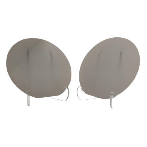 Lithium Tantalate Wafer LT
Optical Crystals
Jmwafer
Diameter [Lithium Tantalate Single-Crystal Substrate LiTaO3/LT (2~6 Inches)]: 2 inch - 50.8mm Diameter [Lithium Tantalate Single-Crystal Substrate LiTaO3/LT (2~6 Inches)]: 3 inch - 76.2mm Diameter [Lithium Tantalate Single-Crystal Substrate LiTaO3/LT (2~6 Inches)]: 4 inch - 100mm
LiTaO₃ Usually Colorless/Pale Yellow,Trigonal Distorted-Perovskite Structure,Excellent Electro-Optic,Piezoelectric/Pyroelectric Properties.
-
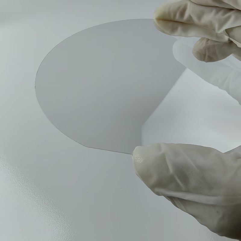 Lithium Niobate Wafer LN
Optical Crystals
Jmwafer
Diameter [Lithium Niobate Single-Crystal Substrate LiNbO3/LN (2~6 Inches)]: 2 inch - 50.8mm Diameter [Lithium Niobate Single-Crystal Substrate LiNbO3/LN (2~6 Inches)]: 3 inch - 76.2mm Diameter [Lithium Niobate Single-Crystal Substrate LiNbO3/LN (2~6 Inches)]: 4 inch - 100mm
LiNbO₃ Trigonal,Good Symmetry/Structural Stability,Piezoelectric,Ferroelectric,Photoelectric,Acousto-Optic/Nonlinear Properties,Curie up to1140℃,High Mechanical Quality/Chemical Stability.
-
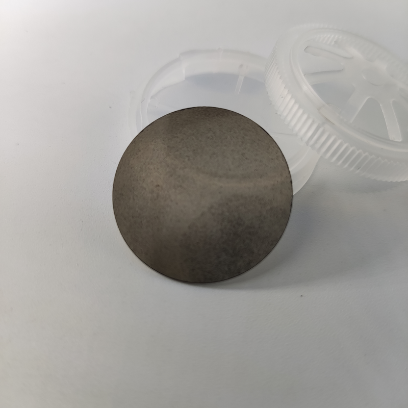 Polycrystalline Diamond
Optical Crystals
Jmwafer
Polycrystalline Diamond - Dimensions: 10 mm × 10 mm Polycrystalline Diamond - Dimensions: 1 inch - 25.4mm Polycrystalline Diamond - Dimensions: 2 inch - 50.8mm
Diamond:Tetrahedrally Packed Carbon,Extremely Hard,Excellent Thermal Conductivity/Broad Optical Transparency,Hardest Known Natural Material,Also Synthesized at High Pressure/Temperature.
-
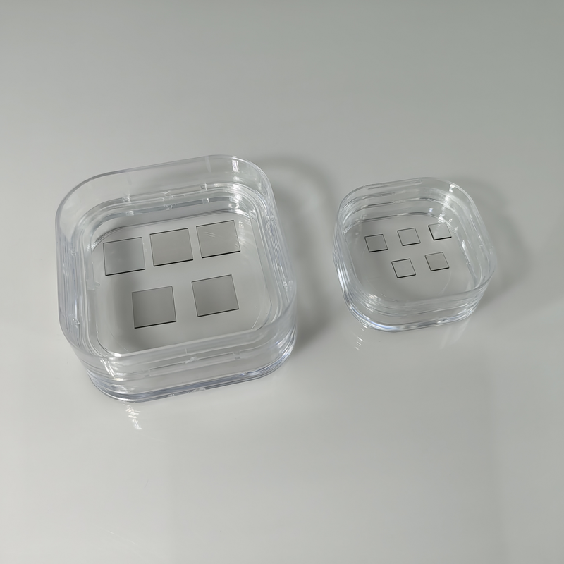 Single-Crystal Diamond
Optical Crystals
Jmwafer
Single-Crystal Diamond - Diameter: 5 mm × 5 mm Single-Crystal Diamond - Diameter: 10 mm × 10 mm Single-Crystal Diamond - Diameter: 20 mm × 20 mm
Diamond:Tetrahedrally Packed Carbon,Extremely Hard,Excellent Thermal Conductivity/Broad Optical Transparency,Hardest Known Natural Material,Also Synthesized at High Pressure/Temperature.
-
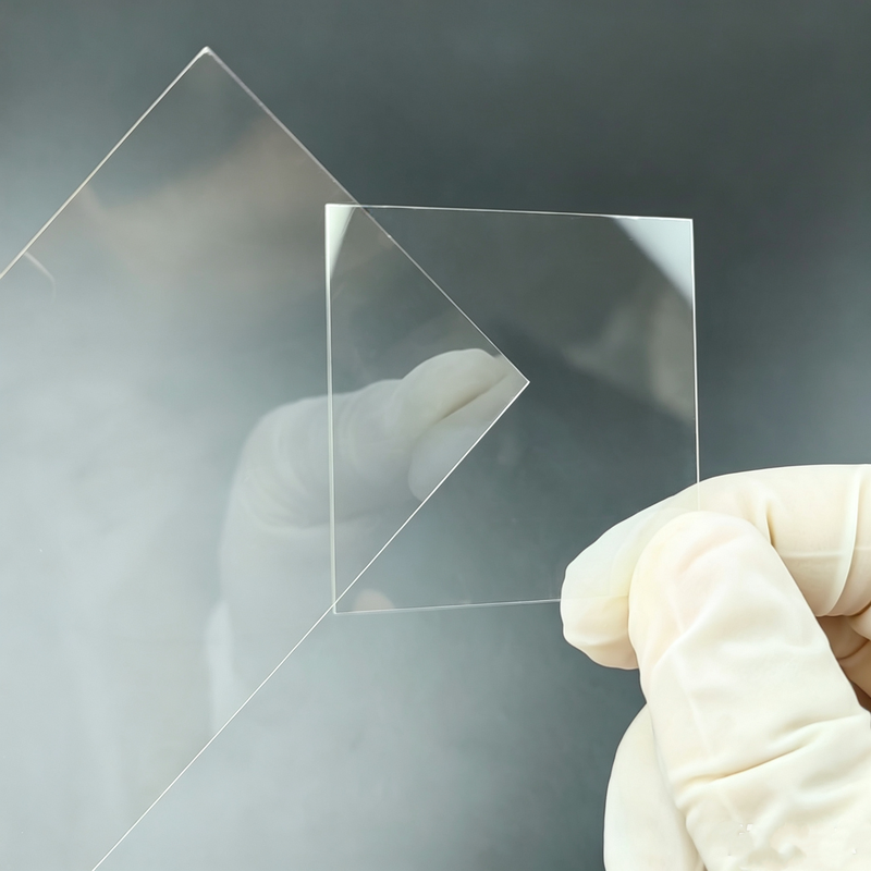 Fluorophlogopite
Optical Crystals
Jmwafer
Fluoromica Substrate - Dimensions: 5 mm × 5 mm Fluoromica Substrate - Dimensions: 10 mm × 10 mm Fluoromica Substrate - Dimensions: 20 mm × 20 mm
Synthetic Fluorophlogopite Mica KMg3(AlSi3O10)F2,Melts1375℃/Long-Term up to1100℃,Colorless Transparent,Strong Acid-Alkali Inert,Stable/Pure/Complete Structure/Flat Cleavage,Easily Split Thin.
Related Articles
The accelerated construction of new‑generation power systems has brought revolutionary upgrades to power‑equipment maintenance workflows.
As fundamental refractive optical components, plano‑convex spherical lenses consist of one convex spherical surface and one flat surface.
Driven by the rapid upgrading of intelligent vehicles, optoelectronic sensing technologies represented by laser sensing and infrared thermal imaging have become core pillars for high-level autonomous driving and smart cockpit iteration. Leveraging automotive-grade optoelectronic R&D advantages, Pilot Technology Group launches the VITAL intelligent vehicle solution. By integrating high-power VCSEL laser chips and vehicle infrared night-vision thermal imagers, the system comprehensively enhances vehicle environmental perception and realizes safer, smarter and more comfortable driving experiences.
As a professional ultraviolet‑laser solution provider, Precilasers has launched its 266 nm narrow‑linewidth industrial laser, delivering reliable single‑frequency output for high‑precision interference lithography, semiconductor inspection and precision metrology applications.
Loading...
Name
Phone
Organization
Use Case

Database Platform