
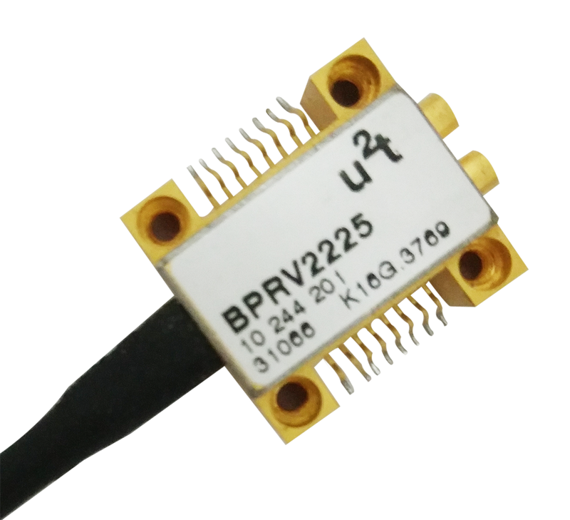
40G Balanced photodetector Balanced Photodetector U2T (Finisar) BPRV2225/ BPRV2125A
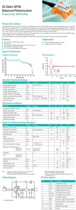
The balanced photoreceiver is double fiber tail fiber input,rate 43Gbps,can be applied to DPSK system;RF interface GPPO,differential output; differential conversion gain 2800V/W,3dB cut-off frequency 31GHz,typical output voltage swing 600mV[BPRV2125A] or 550mV[BPRV2125] under the datasheet conditions. The balanced photoreceiver module BPRV2125(A) is a differential front-end for 43Gbits/s DPSK-applications featuring high differential gain. The photo-receiver module contains two waveguide-integrated PIN photodiode (PD) and a single chip and limiting amplifier (LA) within one small form factor SMD-package. The Receiver is therefore well suited for DPSK and DQPSK applications at 40G and 100G with rates between 20G and 56GBaud. The DC output voltage can be monitored for OUTN and OUTP independently. For each amplifier path a threshold control at a linear amplification stage should be applied to ensure an optimized differential output signal. An excellent electrical and optical phase propagation is achieved by a total skew of lower than 5ps between the balanced signal paths.
 Save to Favorites
Overview
Specifications
| Parameter | Value |
|---|---|
| Storage temperature range T_stg [Absolute Maximum Ratings / Non condensing] | min:-40 °C;max:+85 °C |
| Photo diode bias voltage V_PD1,2 [Absolute Maximum Ratings] | min:0 V;max:+3.5 V |
| Amplifier supply voltage V_EE [Absolute Maximum Ratings] | min:-5.5 V;max:+0.3 V |
| Amplifier adjustment voltage V_ADJ [Absolute Maximum Ratings] | min:-5.5 V;max:+0.3 V |
| Amplifier threshold control voltage V_THCP,N [Absolute Maximum Ratings] | min:-7.0 V;max:+7.0 V |
| Maximum average optical input power P_opt [Absolute Maximum Ratings / NRZ,per input port] | max:9 dBm |
| Electro static discharge V_ESD [Absolute Maximum Ratings / C=100pF,R=1.5kΩ HBM] | min:-500 V;max:500 V |
| Fiber bend radius [Absolute Maximum Ratings] | min:16 mm |
| Operating case temperature range T_case [Operation Conditions] | min:0 °C;max:+75 °C |
| Relative humidity range RH [Operation Conditions / non condensing] | min:5 %;max:85 % |
| Operating wavelength range λ [Operation Conditions] | min:1530 nm;max:1620 nm |
| Average optical input power range P_opt [Operation Conditions / NRZ,per input port] | min:-10 dBm;max:4 dBm |
| Photo diode bias voltage V_PD [Operation Conditions] | min:2.0 V;typical:2.25 V;max:2.75 V |
| Amplifier supply voltage V_EE [Operation Conditions] | min:-5.3 V;typical:-5.2 V;max:-4.8 V |
| Differential conversion gain CG [V_PD1=V_PD2=+2.25V,V_EE=-5.2V,V_adj=-2.4V,λ=1550nm,T=25°C / Measurements performed in single-ended conditions / Measured using Agilent86030A50GHz Lightwave component analyzer] | min:2000 V/W;typical:2800 V/W |
| Photodiode DC responsivity R [V_PD1=V_PD2=+2.25V,V_EE=-5.2V,V_adj=-2.4V,λ=1550nm,T=25°C / optimum polarization] | min:0.5 A/W;typical:0.6 A/W;max:0.75 A/W |
| Polarization dependent loss PDL [V_PD1=V_PD2=+2.25V,V_EE=-5.2V,V_adj=-2.4V,λ=1550nm,T=25°C] | typical:0.4 dB;max:0.6 dB |
| Optical return loss ORL [V_PD1=V_PD2=+2.25V,V_EE=-5.2V,V_adj=-2.4V,λ=1550nm,T=25°C] | min:27 dB;typical:30 dB |
| Bit rate [V_PD1=V_PD2=+2.25V,V_EE=-5.2V,V_adj=-2.4V,λ=1550nm,T=25°C / NRZ,DPSK] | typical:43 Gbit/s |
| 3dB cut-off frequency f_3dB [V_PD1=V_PD2=+2.25V,V_EE=-5.2V,V_adj=-2.4V,λ=1550nm,T=25°C / Measured using Agilent86030A50GHz Lightwave component analyzer] | min:27 GHz;typical:31 GHz |
| Lower frequency cut off f_3dB_L [V_PD1=V_PD2=+2.25V,V_EE=-5.2V,V_adj=-2.4V,λ=1550nm,T=25°C] | max:100 kHz |
| Electrical output reflection coefficient S_22 [V_PD1=V_PD2=+2.25V,V_EE=-5.2V,V_adj=-2.4V,λ=1550nm,T=25°C / f=0.5 to15 (first subrow; no separate frequency unit printed) / Measured using Agilent86030A50GHz Lightwave component analyzer] | max:-10 dB |
| Differential output voltage swing V_out_diff [V_PD1=V_PD2=+2.25V,V_EE=-5.2V,V_adj=-2.4V,λ=1550nm,T=25°C / P_opt≥0dBm / negative CML / Measurements performed in single-ended conditions] | typical:600 mV |
| Pulse width [V_PD1=V_PD2=+2.25V,V_EE=-5.2V,V_adj=-2.4V,λ=1550nm,T=25°C / Input pulse1ps,50MHz,optical power set below saturation level of TIA,test in linear range of receiver] | typical:15 ps;max:25 ps |
| Skew [V_PD1=V_PD2=+2.25V,V_EE=-5.2V,V_adj=-2.4V,λ=1550nm,T=25°C] | typical:1 ps;max:2 ps |
| Equivalent input noise density i_noise [V_PD1=V_PD2=+2.25V,V_EE=-5.2V,V_adj=-2.4V,λ=1550nm,T=25°C] | max:80 pA/√Hz |
| Sensitivity Sens [V_PD1=V_PD2=+2.25V,V_EE=-5.2V,V_adj=-2.4V,λ=1550nm,T=25°C / Measurements performed in single-ended conditions / Evaluated from NRZ BER measurement at40Gbit/s(BER≤10⁻¹²,PRBS2³¹-1,back to back,DPSK)] | typical:-10 dBm |
| Amplifier supply current I_EE [V_PD1=V_PD2=+2.25V,V_EE=-5.2V,V_adj=-2.4V,λ=1550nm,T=25°C] | typical:85 mA;max:100 mA |
| Photodiode dark current I_dark [V_PD1=V_PD2=+2.25V,V_EE=-5.2V,V_adj=-2.4V,λ=1550nm,T=25°C / per PD] | typical:5 nA;max:300 nA |
| Power consumption P_con [V_PD1=V_PD2=+2.25V,V_EE=-5.2V,V_adj=-2.4V,λ=1550nm,T=25°C] | typical:0.45 W;max:0.6 W |
Applications
Key Features
Datasheet
Please provide your email to download the datasheet.
Invalid email format. Please try again.
Supplier Information
Related Products
-
 PD-500B
Optical Detectors
Inxuntech
Center wavelength: 800~1700nm Bandwidth (3dB): 500MHz Common-Mode Rejection Ratio: >25dB
Yingxun Xinguang's balanced photodetection module combines precision symmetrical optics, matched high-frequency InGaAs photodiodes and an ultra-low-noise transimpedance amplifier (TIA). This high-performance module provides high bandwidth and excellent common-mode noise rejection.
-
 Whisper Silicon Solid-State Detector Module
Optical Detectors
Pavilionintegration
Input Supplier Voltage: +/-5V Photoelectric Sensitivity [Typical]: 6.0x10⁷ V/W(Typical) Effective Sensing Srea: Ф1/Ф3mm
As the semiconductor industry advances, solid-state detectors (SSDs), including silicon photomultipliers (SiPMs) and other semiconductor photodetectors, are developing rapidly. Heat-dissipation modules, PCBs, special optics and other functional modules can be added to their configuration for fluorescence detection in life-science instruments, providing excellent performance and reliability. Used together with PIC's innovative, compact, low-noise diode lasers, SiPM detectors support clinical, diagnostic and research applications in moving toward smaller, highly integrated and highly reliable systems.
-
 Whisper Silicon Solid-State Detector Module
Optical Detectors
Pavilionintegration
Input Supplier Voltage: +/-5V Photoelectric Sensitivity [Typical]: 6.0x10⁷ V/W(Typical) Effective Sensing Srea: Ф1/Ф3mm
As the semiconductor industry advances, solid-state detectors (SSDs), including silicon photomultipliers (SiPMs) and other semiconductor photodetectors, are developing rapidly. Heat-dissipation modules, PCBs, special optics and other functional modules can be added to their configuration for fluorescence detection in life-science instruments, providing excellent performance and reliability. Used together with PIC's innovative, compact, low-noise diode lasers, SiPM detectors support clinical, diagnostic and research applications in moving toward smaller, highly integrated and highly reliable systems.
-
 1000um Indium Gallium Arsenide Detector OPD-1-X-X-X-XX-X
Optical Detectors
O-send
Absolute Maximum Ratings - Storage Temperature: -40°C~+100°C Absolute Maximum Ratings - Operating temperature: -40°C~+85°C Absolute Maximum Ratings - Reverse Voltage [CW]: 30V
The 1000um InGaAs detector is mainly used to manufacture power meters. Its detection wavelength ranges from 800nm to 1700nm, and its photosensitive area is 1000um.
-
 2000um Indium Gallium Arsenide Detector Die OTC-PD-2000-TOXX-XX
Optical Detectors
O-send
Responsivity [Vr=-5V]: min:0.70;typical:0.85 Dark current: max:0.7 mA Photosensitive Area Diameter: 2000um
2000μm InGaAs PIN detectors in TO-CAN packages are widely used in the manufacture of optical communication, test and measurement equipment.
Related Articles
Electro-optic deflectors (EODs) are optical devices used to steer or deflect light beams by applying an electric field to a specialized optical crystal. Unlike mechanical beam steering systems that rely on moving mirrors, electro-optic deflectors enable high-speed, non-mechanical beam control with exceptional precision and responsiveness. They are widely used in laser scanning, optical communications, microscopy, laser printing, spectroscopy, and scientific research, where rapid and accurate laser beam positioning is essential.
The 850 nm and 940 nm infrared narrow‑bandpass filters launched by Innovation Photoelectric are core optical components specially designed for day‑and‑night security cameras. They effectively eliminate image interference during visible‑light and infrared‑illumination switching, delivering stable round‑the‑clock monitoring performance.
Within cutting‑edge ultrafast photonics research, asynchronous optical sampling (ASOPS) and synchronous sampling serve as fundamental technologies for terahertz excitation detection, coherent Raman imaging and other time‑resolved spectroscopy experiments.
Shanghai Connet Laser Technology Co., Ltd. focuses on technological innovation, delivering cutting-edge photonic products & solutions for industrial lasers, LiDAR, fiber optic sensing, coherent telecom, cold atom physics and precision spectroscopy research & mass manufacturing.
Loading...
Name
Phone
Organization
Use Case

Database Platform