
Wavelength-tunable laser CW Tunable Laser Full C Band Butterfly Package Finisar S7500 F7500
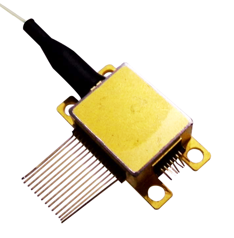
Finisar’s S7500 tunable laser incorporates a monolithic InP chip that integrates a tunable MG-Y laser with a semiconductor optical amplifier (SOA). The MG-Y (Modulated Grating Y-branch) laser is an electronically tuned device that can address any wavelength in the C-band. Since no mechanical or thermal adjustments are necessary, channel switching is very fast. The SOA facilitates flexible control of the output power and acts as a shutter when reverse biased, enabling dark tuning between channels. The devices are packaged into a compact, low-profile hermetically sealed package, with an internal optical isolator and a wavelength locker. The locker monitors both output power and frequency of the light emitted from the chip, enabling a closed loop control that guarantees stability of the frequency and output power over life, to within the requirements of 50 GHz ITU grid spacing applications. The S7500 is provided with polarization maintaining fiber for use with an external modulator. The laser is RoHS compliant and lead free per Directive 2011/65/EU.
 Save to Favorites
Overview
Specifications
| Parameter | Value |
|---|---|
| Storage temperature T_S [Absolute Maximum Ratings] | min:-40 °C;max:85 °C |
| Relative humidity RH [Absolute Maximum Ratings / Non-condensing] | min:0 %;max:85 % |
| Laser diode reverse voltage (all sections) [Absolute Maximum Ratings] | max:3 V |
| Laser gain current I_g [Absolute Maximum Ratings] | max:160 mA |
| Reflector currents I_rl, I_rr [Absolute Maximum Ratings] | max:50 mA |
| Phase current I_pc [Absolute Maximum Ratings] | max:10 mA |
| SOA current I_SOA [Absolute Maximum Ratings] | max:240 mA |
| Photodiode bias voltage V_PD,ref, V_PD,λ [Absolute Maximum Ratings] | min:-5 V;max:0 V |
| Photodiode reverse current I_PD,ref, I_PD,λ [Absolute Maximum Ratings] | max:2 mA |
| TEC current I_TEC [Absolute Maximum Ratings] | max:1.2 A |
| TEC voltage V_TEC [Absolute Maximum Ratings] | max:3.5 V |
| Operating case temperature T_OP | min:-5 °C;max:75 °C |
| Laser chip temperature T_L | min:25 °C;max:30 °C |
| Laser gain current I_g | typical:98 mA;max:100 mA |
| Reflector currents (left, right) I_rl, I_rr | max:33 mA |
| Phase current I_pc | max:7.5 mA |
| SOA current I_SOA | typical:90 mA;max:167 mA |
| Photodiode bias voltage V_PD,ref, V_PD,λ | min:-3 V;max:0 V |
| Thermistor resistance R_th [With the laser chip temperature set to 25°C.] | typical:10 kΩ |
| Thermistor sensitivity index β [With the laser chip temperature set to 25°C.] | typical:3930 K |
| TEC current I_TEC [In steady state, with the laser chip temperature set to 25°C, and a case temperature of 75°C.] | typical:<0.75 A;max:0.85 A |
| TEC voltage V_TEC [In steady state, with the laser chip temperature set to 25°C, and a case temperature of 75°C.] | typical:<2.5 V;max:2.8 V |
| Total power dissipation P_tot [In steady state, with the laser chip temperature set to 25°C, and a case temperature of 75°C.] | typical:<2.2 W;max:2.8 W |
| Output power P_max [T_OP=-5 to75°C / For all channels, BOL.] | min:13 dBm |
| Output power variation over life ΔP [T_OP=-5 to75°C / With closed loop control on SOA current to maintain a fixed reference PD current.] | min:-0.5 dB;max:0.5 dB |
| Output power adjustment range [T_OP=-5 to75°C / Range over which the output power can be adjusted by changing the SOA current, down from the output power P_max, while maintaining all other optical specifications.] | min:4 dB |
| Output power when disabled [T_OP=-5 to75°C / Output power with reverse biased SOA; used in order to block the laser output, e.g. while tuning to another channel.] | max:-35 dBm |
| Lowest emission frequency ν_min [T_OP=-5 to75°C] | min:191.15 THz;typical:191.70 THz |
| Highest emission frequency ν_max [T_OP=-5 to75°C] | typical:196.10 THz;max:196.25 THz |
| Lowest emission wavelength λ_min [T_OP=-5 to75°C] | min:1527.6 nm;typical:1528.8 nm |
| Highest emission wavelength λ_max [T_OP=-5 to75°C] | typical:1563.9 nm;max:1568.4 nm |
| Channel spacing (ITU grid) [T_OP=-5 to75°C] | typical:50 GHz |
| Number of channels | min: 89 |
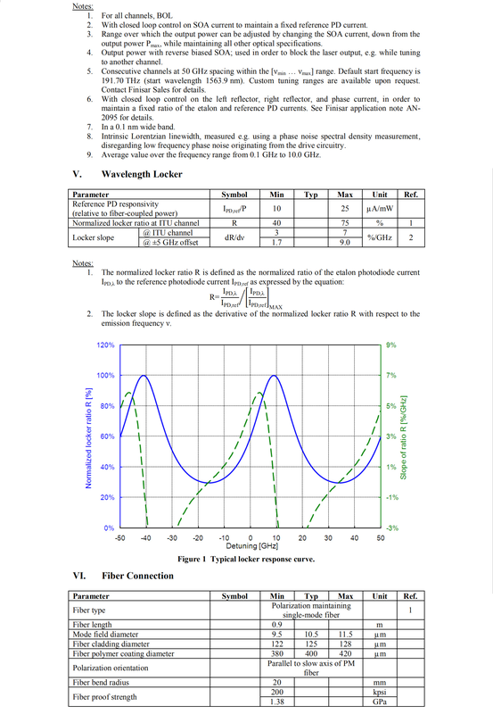
| Frequency accuracy Δν [T_OP=-5 to75°C / With closed loop control on the left reflector, right reflector and phase current, in order to maintain a fixed ratio of the etalon and reference PD currents. See Finisar application note AN-2095 for details.] | min:-2.5 GHz;max:2.5 GHz |
| Side-mode suppression ratio SMSR [T_OP=-5 to75°C] | min:40 dB |
| Optical signal-to-noise ratio OSNR [T_OP=-5 to75°C / In a 0.1nm wide band.] | min:50 dB;typical:55 dB |
| Linewidth LW [T_OP=-5 to75°C / Intrinsic Lorentzian linewidth, measured e.g. using a phase noise spectral density measurement, disregarding low frequency phase noise originating from the drive circuitry.] | max:5 MHz |
| Relative intensity noise RIN [T_OP=-5 to75°C / Average value over the frequency range from0.1GHz to10.0GHz.] | max:-140 dB/Hz |
| Back reflection tolerance [T_OP=-5 to75°C] | max:-14 dB |
| Optical isolation [T_OP=-5 to75°C] | min:40 dB |
| Polarization extinction ratio PER [T_OP=-5 to75°C] | min:20 dB |
| Reference PD responsivity (relative to fiber-coupled power) I_PD,ref/P | min:10 µA/mW;max:25 µA/mW |
| Normalized locker ratio at ITU channel R [The normalized locker ratio R is the ratio of the etalon photodiode current I_PD,λ to the reference photodiode current I_PD,ref, normalized by its maximum: R=(I_PD,λ/I_PD,ref)/[I_PD,λ/I_PD,ref]_MAX.] | min:40 %;max:75 % |
| Locker slope dR/dν [@ITU channel / The locker slope is defined as the derivative of the normalized locker ratio R with respect to the emission frequency ν.] | min:3 %/GHz;max:7 %/GHz |
| Locker slope dR/dν [@±5GHz offset / The locker slope is defined as the derivative of the normalized locker ratio R with respect to the emission frequency ν.] | min:1.7 %/GHz;max:9.0 %/GHz |
| Fiber type [Fujikura SM15-PS-U40A-H PANDA or equivalent.] | Polarization maintaining single-mode fiber |
| Fiber length | min:0.9 m |
| Mode field diameter | min:9.5 µm;typical:10.5 µm;max:11.5 µm |
| Fiber cladding diameter | min:122 µm;typical:125 µm;max:128 µm |
| Fiber polymer coating diameter | min:380 µm;typical:400 µm;max:420 µm |
| Polarization orientation | Parallel to slow axis of PM fiber |
| Fiber bend radius | min:20 mm |
| Fiber proof strength | min: 200 kpsi / 1.38 GPa |
Applications
Key Features
Datasheet
Please provide your email to download the datasheet.
Invalid email format. Please try again.
Supplier Information
Related Products
-
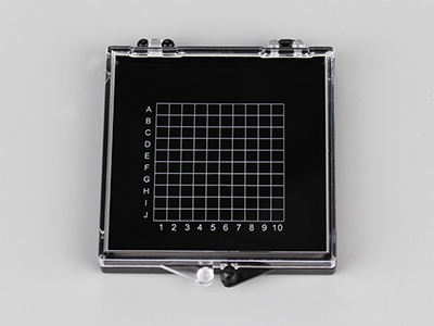 HX5510-BT-100-2
Packages
Meige-sy
Type: Silicone Adhesive with High, Medium or Low Tack Available Specifications: Internal Wire-Mesh Pattern Customizable Material: Ordinary plastic or antistatic plastic selectable
-
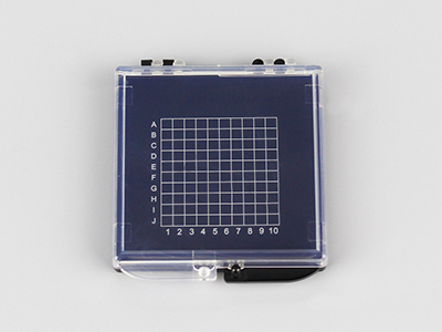 HX5510-BT-100-3
Packages
Meige-sy
-
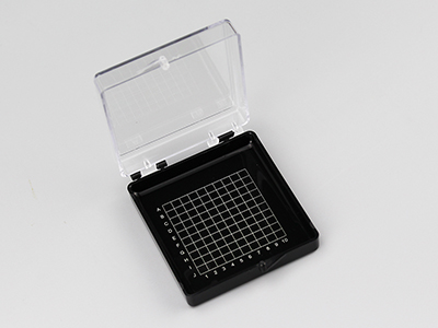 HX6620-BT-100-3
Packages
Meige-sy
Type: Silicone Adhesive with High, Medium or Low Tack Available Specifications: Internal Wire-Mesh Pattern Customizable Material: Ordinary plastic or antistatic plastic selectable
-
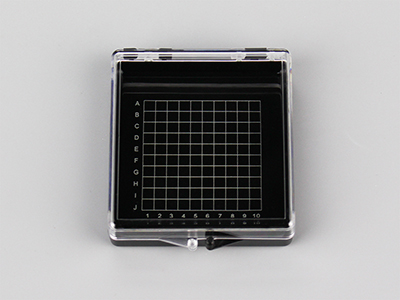 HX6620-BT-100-4
Packages
Meige-sy
-
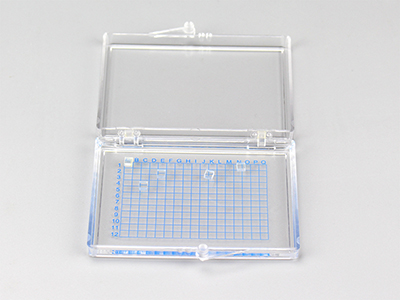 HX8515-TT-204
Packages
Meige-sy
Related Articles
Electro-optic deflectors (EODs) are optical devices used to steer or deflect light beams by applying an electric field to a specialized optical crystal. Unlike mechanical beam steering systems that rely on moving mirrors, electro-optic deflectors enable high-speed, non-mechanical beam control with exceptional precision and responsiveness. They are widely used in laser scanning, optical communications, microscopy, laser printing, spectroscopy, and scientific research, where rapid and accurate laser beam positioning is essential.
The 850 nm and 940 nm infrared narrow‑bandpass filters launched by Innovation Photoelectric are core optical components specially designed for day‑and‑night security cameras. They effectively eliminate image interference during visible‑light and infrared‑illumination switching, delivering stable round‑the‑clock monitoring performance.
Within cutting‑edge ultrafast photonics research, asynchronous optical sampling (ASOPS) and synchronous sampling serve as fundamental technologies for terahertz excitation detection, coherent Raman imaging and other time‑resolved spectroscopy experiments.
Shanghai Connet Laser Technology Co., Ltd. focuses on technological innovation, delivering cutting-edge photonic products & solutions for industrial lasers, LiDAR, fiber optic sensing, coherent telecom, cold atom physics and precision spectroscopy research & mass manufacturing.
Loading...
Name
Phone
Organization
Use Case

Database Platform