
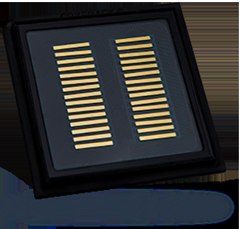
High-Power Semiconductor Laser Bar Chip -976nm-300W-CW
 Save to Favorites
Specifications
| Parameter | Value |
|---|---|
| Center wavelength λ_c [25°C] | Min :966 nm; Typical :976 nm; Max :986 nm |
| Output Power P_opt [25°C] | Typical :300 W |
| Operating mode [25°C] | Typical :CW/QCW |
| Number of Emitting Units [25°C] | Typical :62 |
| Emitting Region Width W [25°C] | Typical :120 μm |
| Emission Spot Period P [25°C] | Typical :150 μm |
| Fill factor F [25°C] | Typical :80 % |
| Bar Length B [25°C] | Min :9900 μm; Typical :10000 μm; Max :10100 μm |
| Cavity length L [25°C] | Min :1480 μm; Typical :1500 μm; Max :1520 μm |
| Thickness D [25°C] | Min :125 μm; Typical :135 μm; Max :145 μm |
| Threshold current Iₜₕ [25°C] | Typical :25 A; Max :30 A |
| Operating current Iₒₚ [25°C] | Typical :300 A |
| Operating voltage Vₒₚ [25°C] | Typical :1.5 V; Max :1.6 V |
| Spectral width △λ [25°C;FWHM] | Typical :4 nm |
| Slope efficiency η [25°C] | Min :1.08 W/A; Typical :1.12 W/A |
| Polarization [25°C] | Typical :TE |
| Operating temperature [25°C] | Typical :25 °C |
Applications
Key Features
Datasheet
Supplier Information
Related Products
-
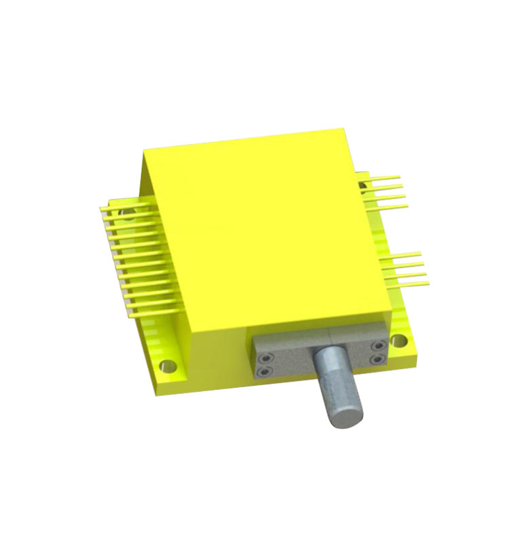 C Series High-Power Semiconductor Laser
Laser Diodes
Tc-semi
Output Power [25℃]: Typical:15 W Center wavelength [25℃]: Typical:1550±10 Spectral Width (90% Energy) [25℃]: Typical:<10.0 nm
-
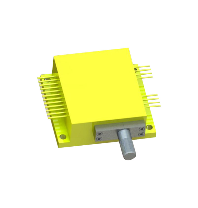 G Series High-Power Semiconductor Laser
Laser Diodes
Tc-semi
Output Power [25℃]: Typical:5 W Center wavelength [25℃]: Typical:1550±10 Spectral Width (90% Energy) [25℃]: Typical:<6.0 nm
-
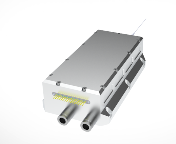 V Series High-Power Semiconductor Laser
Laser Diodes
Tc-semi
Output Power [20℃]: Typical:70 W Center wavelength [20℃]: Typical:520±10 Spectral width (FWHM) [20℃]: Typical:<6.0
-
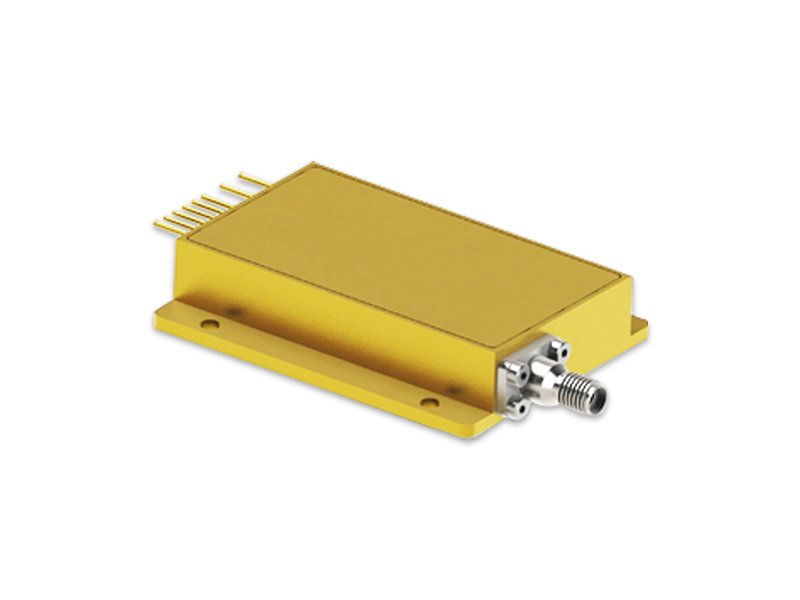 D Series High-Power Semiconductor Laser
Laser Diodes
Tc-semi
Output Power [25℃]: Typical:120 W Center wavelength [25℃]: Typical:878.6±0.5 Spectral width (FWHM) [25℃]: Typical:<0.5 nm
-
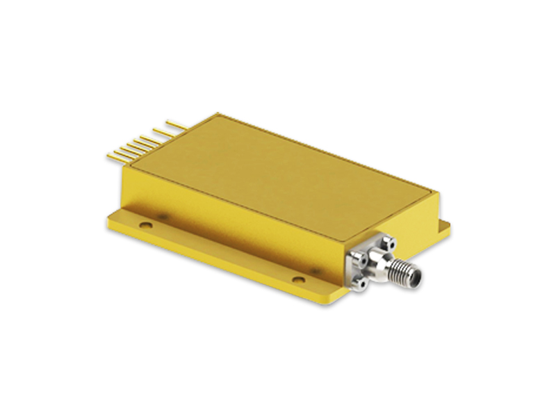 T-Series Laser Diode Module
Laser Diodes
Tc-semi
Output Power [25℃]: Typical:30 W Center Wavelength [25℃]: Min:878.1 nm;Max:879.1 nm Spectral Width (FWHM) [25℃]: Typical:<0.5 nm
Related Articles
An infrared transmitter (IR transmitter) is a basic electronic component that sends invisible infrared light signals for short-range wireless control. It is widely used in daily electronics, smart home devices, and industrial equipment due to its low cost, low power consumption, and stable performance.
As a vital emerging sector of modern three-dimensional spatial economy, the low-altitude economy has become a new global growth driver. It covers a wide range of commercial scenarios, including UAV navigation and obstacle avoidance, precise airspace management, aerial mapping, low-altitude logistics distribution, security monitoring and emergency disaster rescue. Nevertheless, frequent extreme weather, complex terrain obstacles and increasingly dense low-altitude flight activities pose severe challenges to the safety and stability of low-altitude aircraft operations.
Widely adopted in small home appliances, industrial instruments, smart toys and atomization devices, the 0603 patch emerald green LED serves as a core status-indicating optical component.
Founded in 2004, Wuhan Union Optic Inc. is a National Specialized, Refined, Unique & Innovative "Little Giant" high-tech enterprise located in Wuhan East Lake High-Tech Development Zone.
Loading...
Name
Phone
Organization
Use Case

Database Platform