
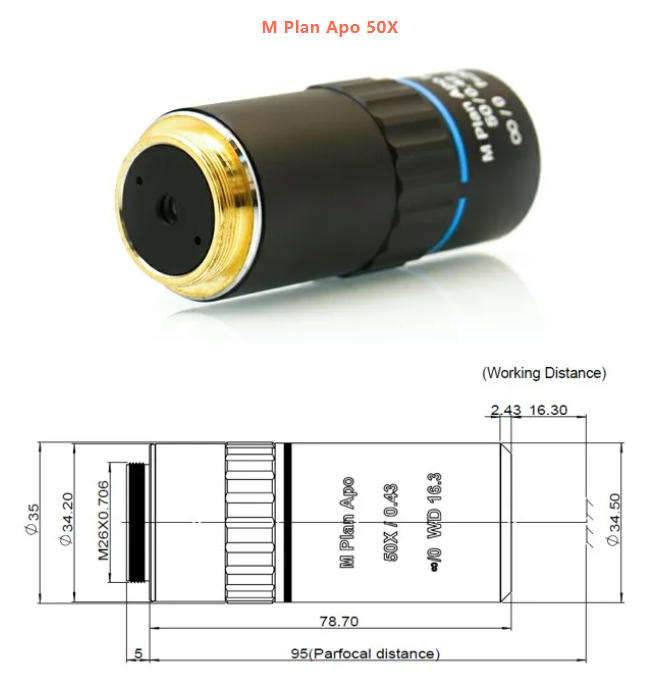
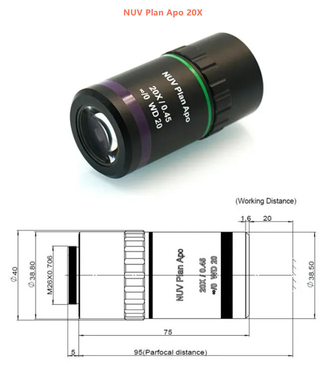
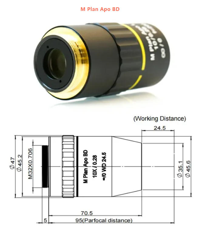
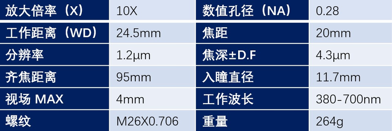
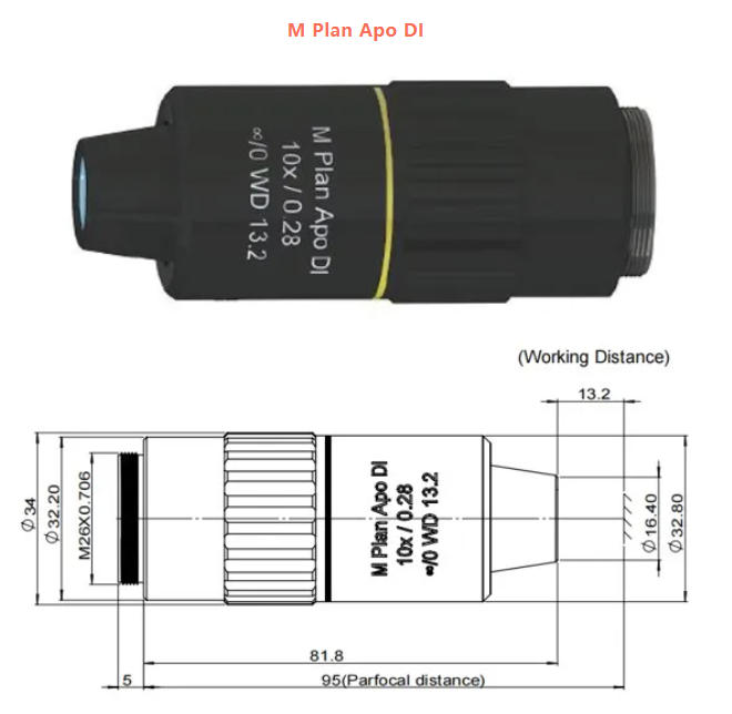
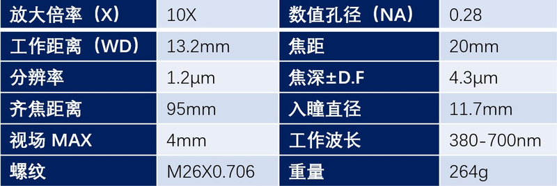
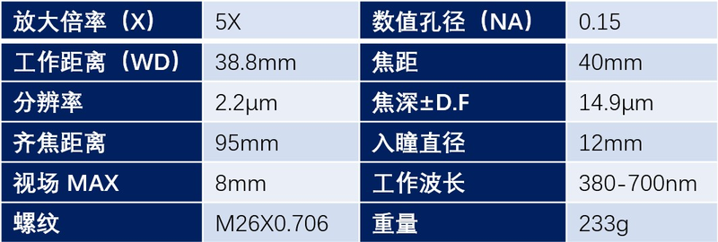
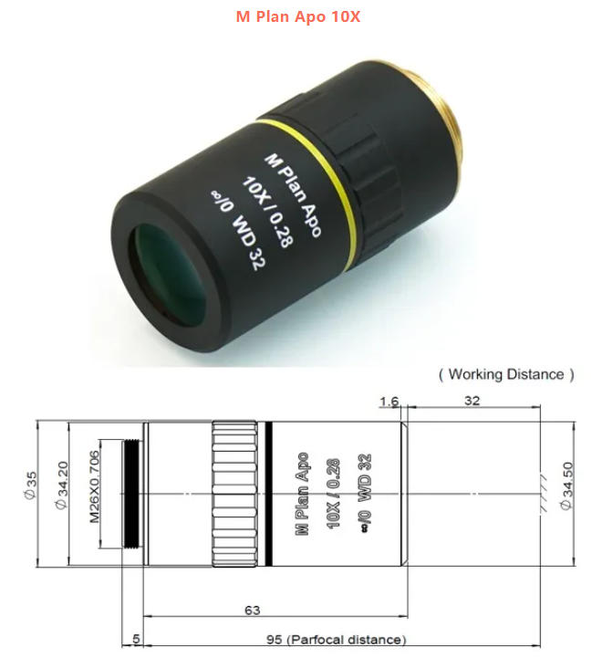
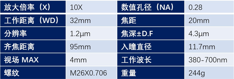
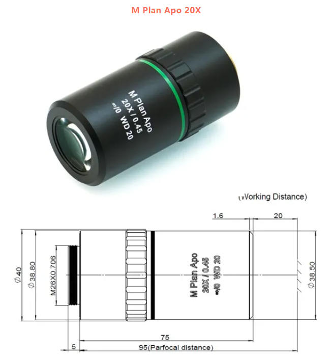
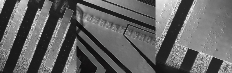
Large field-of-view industrial microscope objective (M Plan Apo 2X)
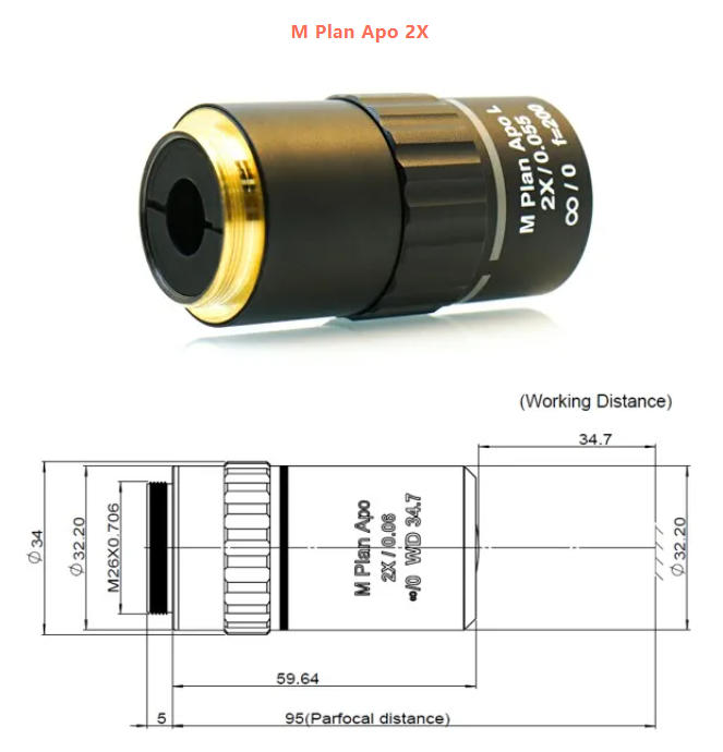
The Wavelength Optoelectronics large field-of-view industrial microscope objective is made of high-quality optical glass and combined with anti-reflection coating technology, significantly improving light transmission efficiency. With a plan apochromatic design, the imaging details are clear and the contrast is high. The objective is designed based on an infinite conjugate optical system, with a parfocal distance of 95mm, and is a brightfield objective for coaxial illumination. For large field-of-view image observation, it supports up to an image-side diameter of 40mm, facilitating the integration of various accessories and adaptation to complex working conditions. It can be widely used in precision metrology and inspection in the semiconductor field as well as high-precision visual analysis and quality monitoring in various industrial scenarios.
 Save to Favorites
Overview
Specifications
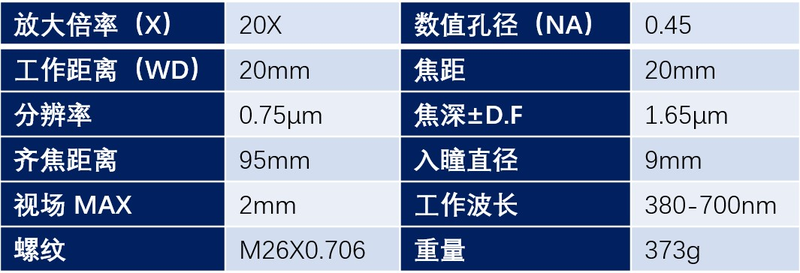
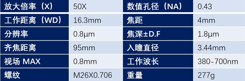
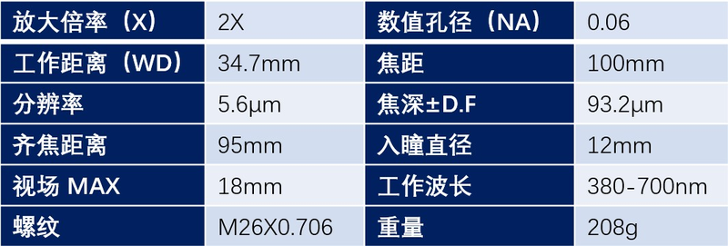
| Parameter | Value |
|---|---|
| Magnification (X) | 2X |
| Working distance (WD) | 34.7 mm |
| Resolution | 5.6 μm |
| Parfocal distance | 95 mm |
| Field of view MAX | 18 mm |
| Thread | M26X0.706 |
| Numerical aperture (NA) | 0.06 |
| Focal Length | 100 mm |
| Depth of focus ±D.F | 93.2 μm |
| Entrance pupil diameter | 12 mm |
| Operating Wavelength | 380-700nm |
| Weight | 208 g |
Applications
Key Features
Datasheet
Please provide your email to download the datasheet.
Invalid email format. Please try again.
Supplier Information
Related Products
-
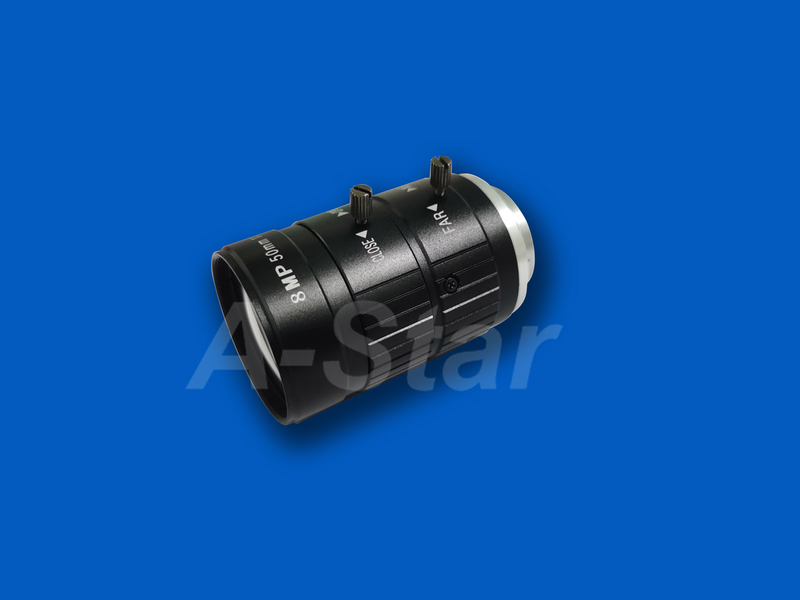 Line-scan lens
Imaging Lenses and Objectives
Astarphotonics
Focal length [Resolution(Pixel):4K / Relative aperture:F2.8 / Mount:M42X1 / Image format(“):Φ43mm / Field of view(°):53]: 25mm Resolution Pixel [Focal length(mm):25mm / Relative aperture:F2.8 / Mount:M42X1 / Image format(“):Φ43mm / Field of view(°):53]: 4K Relative aperture [Focal length(mm):25mm / Resolution(Pixel):4K / Mount:M42X1 / Image format(“):Φ43mm / Field of view(°):53]: F2.8
Line-scan lenses are machine-vision lenses mainly used for production-line inspection, including pharmaceutical fill-level and label inspection, date and batch-code reading, safety-seal inspection and dimensional consistency checks. Chenzheng Optoelectronics provides various line-scan lens designs and customization.
-
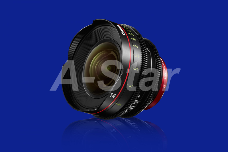 Digital camera lens
Imaging Lenses and Objectives
Astarphotonics
Focal length [Relative aperture:1:1.8 / Mount:Various options available / Image format(“):APS-C Half-frame / Horizontal field of view(°):51°]: 25mm Relative aperture [Focal length(mm):25mm / Mount:Various options available / Image format(“):APS-C Half-frame / Horizontal field of view(°):51°]: 1:1.8 Interface Mount [Focal length(mm):25mm / Relative aperture:1:1.8 / Image format(“):APS-C Half-frame / Horizontal field of view(°):51°]: Various options available
Chenzheng Optoelectronics produces various digital-camera lenses and provides lens design and customization.
-
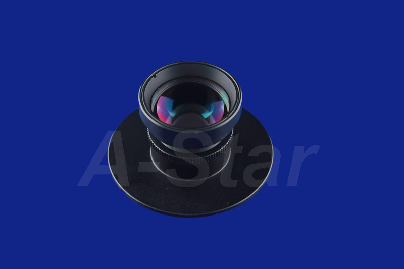 UAV aerial imaging lens
Imaging Lenses and Objectives
Astarphotonics
Focal length [Resolution(Pixel):35MP / Relative aperture:1:5.6 / Mount:SONY NEX-E / Image format(“):APS-C half-frame / Horizontal field of view(°):51]: 25mm Resolution Pixel [Focal length(mm):25mm / Relative aperture:1:5.6 / Mount:SONY NEX-E / Image format(“):APS-C half-frame / Horizontal field of view(°):51]: 35MP Relative aperture [Focal length(mm):25mm / Resolution(Pixel):35MP / Mount:SONY NEX-E / Image format(“):APS-C half-frame / Horizontal field of view(°):51]: 1:5.6
UAV aerial-photography lenses, also called surveying lenses, support aerial imaging, mapping and geological surveys. Chenzheng's lenses feature ultralow distortion, high-transmission multilayer coatings, lightweight construction and ED glass. Various designs and customization are available.
-
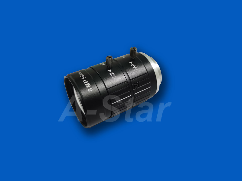 Machine vision lens
Imaging Lenses and Objectives
Astarphotonics
Focal length [Resolution (Pixel) :8MP / Relative aperture :1:2.8 / Mount :C / Image format (“):1/1.8 / Horizontal field of view Horizontal field view(°):18]: 25mm Resolution Pixel [Focal length Focal length(mm):25mm / Relative aperture :1:2.8 / Mount :C / Image format (“):1/1.8 / Horizontal field of view Horizontal field view(°):18]: 8MP Relative aperture [Focal length Focal length(mm):25mm / Resolution (Pixel) :8MP / Mount :C / Image format (“):1/1.8 / Horizontal field of view Horizontal field view(°):18]: 1:2.8
Machine-vision lenses inspect products on production lines, including electronic-component defects, batch numbers, manufacturing dates and expiry dates. Chenzheng's lenses offer large image formats, 4K resolution, ultralow distortion and high-transmission multilayer broadband coatings, designed for automated factory lines. Various types are available.
-
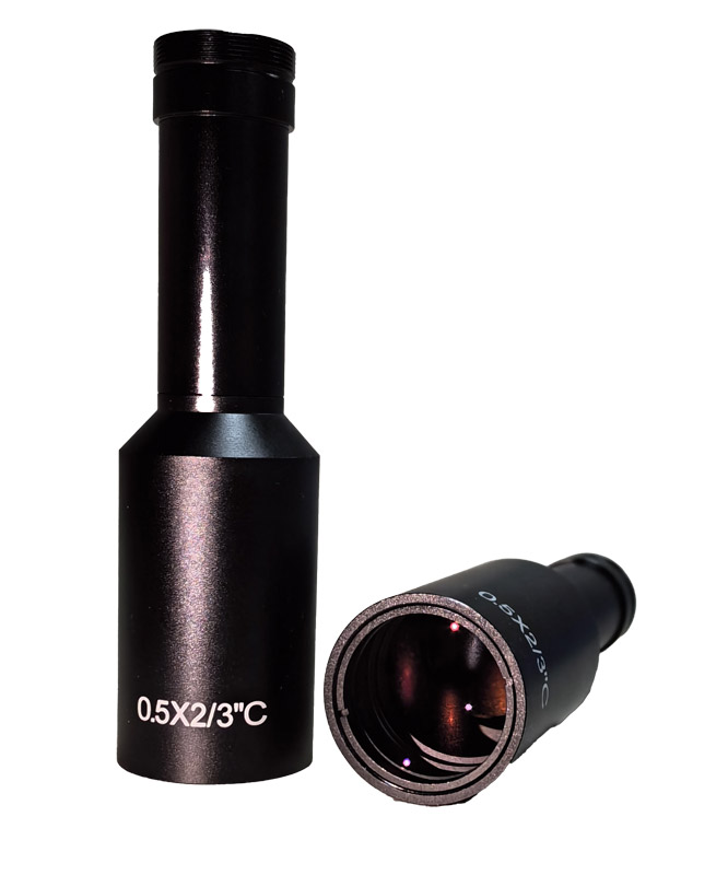 Telecentric lens (Telecentric)
Imaging Lenses and Objectives
Astarphotonics
Operating Wavelength: 400 – 700nm Optical magnification: 0.5X Working distance: 110mm±3%
Telecentric lenses correct parallax in conventional industrial lenses by maintaining constant magnification over a specified object-distance range, particularly useful when measured objects lie in different planes. This lens combines excellent telecentricity and low distortion with a fixed aperture and lockable focus for stable performance in measurement systems, workshops and assembly lines.
Related Articles
Electro-optic deflectors (EODs) are optical devices used to steer or deflect light beams by applying an electric field to a specialized optical crystal. Unlike mechanical beam steering systems that rely on moving mirrors, electro-optic deflectors enable high-speed, non-mechanical beam control with exceptional precision and responsiveness. They are widely used in laser scanning, optical communications, microscopy, laser printing, spectroscopy, and scientific research, where rapid and accurate laser beam positioning is essential.
The 850 nm and 940 nm infrared narrow‑bandpass filters launched by Innovation Photoelectric are core optical components specially designed for day‑and‑night security cameras. They effectively eliminate image interference during visible‑light and infrared‑illumination switching, delivering stable round‑the‑clock monitoring performance.
Within cutting‑edge ultrafast photonics research, asynchronous optical sampling (ASOPS) and synchronous sampling serve as fundamental technologies for terahertz excitation detection, coherent Raman imaging and other time‑resolved spectroscopy experiments.
Shanghai Connet Laser Technology Co., Ltd. focuses on technological innovation, delivering cutting-edge photonic products & solutions for industrial lasers, LiDAR, fiber optic sensing, coherent telecom, cold atom physics and precision spectroscopy research & mass manufacturing.
Loading...
Name
Phone
Organization
Use Case

Database Platform