
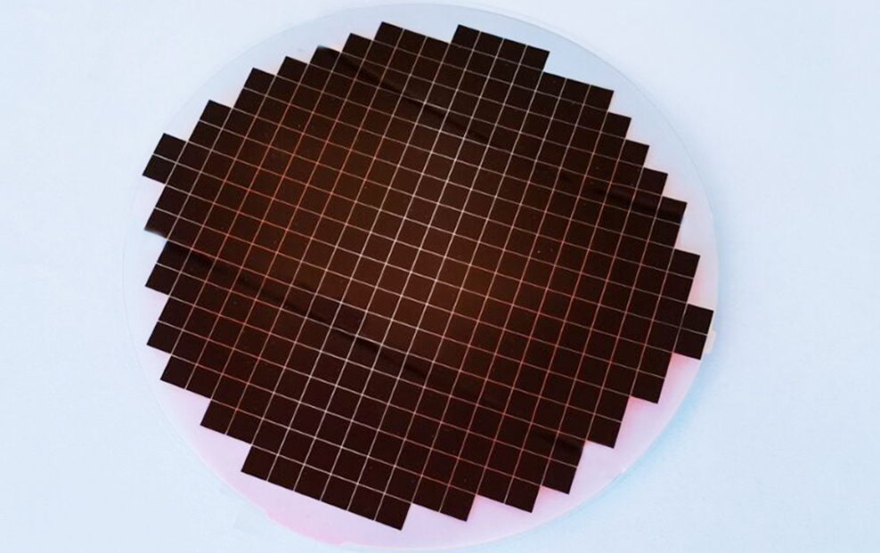
Lithography Wafer
Lithography Wafer_Semiconductor Applications_Products_Zhejiang Lante Optics Co., Ltd. Process Capability and Accuracy Photoresist coating Spin coating Thickness accuracy ≤3% (for flat surfaces) Spray coating Thickness accuracy ≤10% (for flat/convex-concave surfaces) Lithography Accuracy 2um Overlay accuracy: 0.15um Development Accuracy 2um Development uniformity <5% Etching Dimensional variation ±1um Lithography Wafer_Semiconductor Applications_Products_Zhejiang Lante Optics Co., Ltd. Lante Optics LANTE OPTICS About Us Company Profile Chairman's Message Corporate Culture Development History Corporate Honors Products Traditional Optics Prisms Lenses Filters Optical Communications Medical Applications Micro Prisms Micro Glass Spherical/Aspherical Lenses Automotive Applications Automotive Rearview Mirror Applications Logo Projection Lamp Applications Vehicle-Mounted Lens Applications Semiconductor Applications Substrate Wafers Carrier Wafers Packaging Wafers Through-Glass-Via Wafers (TGV) Lithography Wafers Consumer Electronics Micro Prisms Small Lenses PBS Prisms Lithography Glass Precision Glass Molding Glass Aspherical Lenses Laser Collimating Lenses FAC Lenses 5G Optical Communication Lenses Lens Design & Assembly Vehicle-Mounted Lenses Projection Lenses TOF Lenses Low-Light Lenses Special-Industry Lenses MLA Microlens Array MLA Microlens Array - Welcome Light Carpet / Lightcarpet MLA Microlens Array - Headlamps / Headlamps MLA Microlens Array - Ambient Light / Interior Projection MLA Microlens Array - Safety Indication Projection System / Safety Projection Technical Strength Production Equipment Inspection Equipment Environmental Test Equipment Research & Development Innovation Achievements News Center Company News Company Announcements Industry News Group Announcements Talent Recruitment Talent Philosophy Work Environment Job Openings Investor Relations Investor Relations Management Real-Time Quotes Company Announcements Interactive Platform Contact Us Contact Information Message Feedback Chinese ENGLISH Chinese ENGLISH 01 About Us Company Profile Chairman's Message Corporate Culture Development History Corporate Honors 02 Products Traditional Optics Optical Communications Medical Applications Automotive Applications Semiconductor Applications Consumer Electronics Precision Glass Molding Lens Design & Assembly MLA Microlens Array 03 Technical Strength Production Equipment Inspection Equipment Environmental Test Equipment Research & Development Innovation Achievements 04 News Center Company News Company Announcements Industry News Group Announcements 05 Talent Recruitment Talent Philosophy Work Environment Job Openings 06 Investor Relations Investor Relations Management Real-Time Quotes Company Announcements Interactive Platform 07 Contact Us Contact Information Message Feedback Website Home About Us Company Profile Chairman's Message Corporate Culture Development History Corporate Honors Products Traditional Optics Optical Communications Medical Applications Automotive Applications Semiconductor Applications Consumer Electronics Precision Glass Molding Lens Design & Assembly MLA Microlens Array Technical Strength Production Equipment Inspection Equipment Environmental Test Equipment Research & Development Innovation Achievements News Center Company News Company Announcements Industry News Group Announcements Talent Recruitment Talent Philosophy Work Environment Job Openings Investor Relations Investor Relations Management Real-Time Quotes Company Announcements Interactive Platform Contact Us Contact Information Message Feedback ENGLISH Website Home > Products > Semiconductor Applications > Lithography Wafer Lithography Wafer "> Lithography Wafer "> Technical Specifications Display Process Capability and Accuracy Photoresist Coating Spin Coating Thickness Accuracy ≤3% (for flat surfaces) Photoresist Coating Spray Coating Thickness Accuracy ≤10% (for flat/convex-concave surfaces) Lithography Accuracy 2um Overlay Accuracy: 0.15um Development Accuracy 2um Development Uniformity <5% Etching Dimensional Variation ±1um Product Inquiry Name: Tel: Email: Inquiry Content: Can't read, try another * Please fill in the form carefully. Inquiry responses are handled during working hours: Monday to Friday, 9:00 to 18:00. Please wait patiently for our reply. About Us Company Profile Chairman's Message Corporate Culture Development History Corporate Honors Products Traditional Optics Optical Communications Medical Applications Automotive Applications Semiconductor Applications Consumer Electronics Precision Glass Molding Lens Design & Assembly MLA Microlens Array Technical Strength Production Equipment Inspection Equipment Environmental Test Equipment Research & Development Innovation Achievements News Center Company News Company Announcements Industry News Group Announcements Talent Recruitment Talent Philosophy Work Environment Job Openings Investor Relations Investor Relations Management Real-Time Quotes Company Announcements Interactive Platform Contact Us Contact Information Message Feedback Lante Optics LANTE OPTICS WeChat Official Account Official Mobile Site COPYRIGHT 2020 Zhejiang Lante Optics Co., Ltd. Technical Support: Website Filing/License No.: ICP 16015954-1 Back to Top
 Save to Favorites
Overview
Specifications
| Parameter | Value |
|---|---|
| Photoresist Spin Coating | Adhesive thickness accuracy ≤3% (applicable to flat surfaces) |
| Photoresist Spray Coating | Adhesive thickness accuracy ≤10% (applicable to flat/convex/concave surfaces) |
| Lithography | Accuracy 2 um, registration accuracy: 0.15 um |
| Development | Accuracy 2 um, development uniformity <5% |
| Etching | Dimension variation ±1um |
Applications
Datasheet
Please provide your email to download the datasheet.
Invalid email format. Please try again.
Supplier Information
Related Products
-
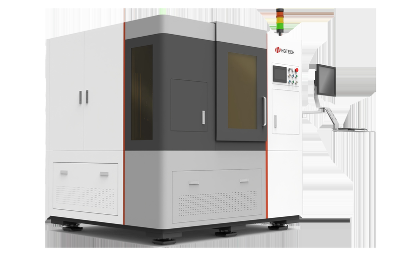 Smart equipment for TGV glacial plate drilling
Ceramic and Glass Components
Hglaser
Smart equipment for TGV glacial plate drilling
Ceramic and Glass Components
Hglaser
Average output power: >20W Process performance: min: 30μm Specification of electricity supply: 220V/50HZ/8KW
TGV (Through Glass Via), a glass perforation device; a combination of laser-induced modifications and chemical etching; and the formation of a massive perforated structure inside the glass. Extensively used in chip wrapping and glass base plate processing Medium
-
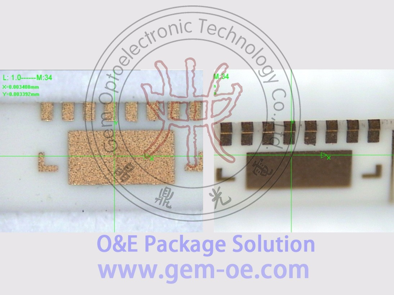 submount
Ceramic and Glass Components
Gem-oe
submount
Ceramic and Glass Components
Gem-oe
Side metalification; product size 2.825*1* 0.127; unit mm; small size; 0.3*1* 0.127. Horizontal and vertical face-to-face accuracy > 5 μm
-
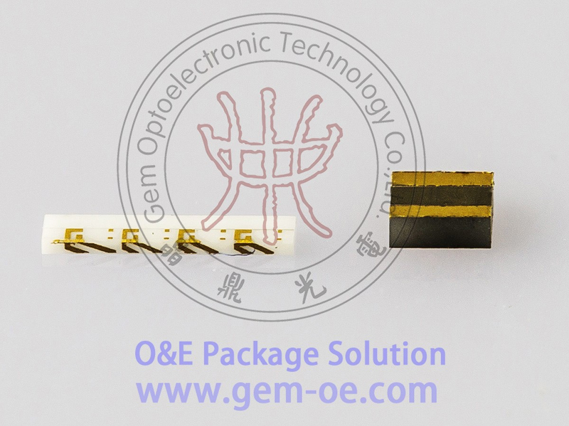 Hot
Ceramic and Glass Components
Gem-oe
Hot
Ceramic and Glass Components
Gem-oe
Lined on thermal deposition; metalted surfaces to Ti, Pt, Au, Cr, Cu, Sn, Ag or Ausn welds, etc.; thickness and composition can be customised
-
 Membrane circuit
Ceramic and Glass Components
Gem-oe
Membrane circuit
Ceramic and Glass Components
Gem-oe
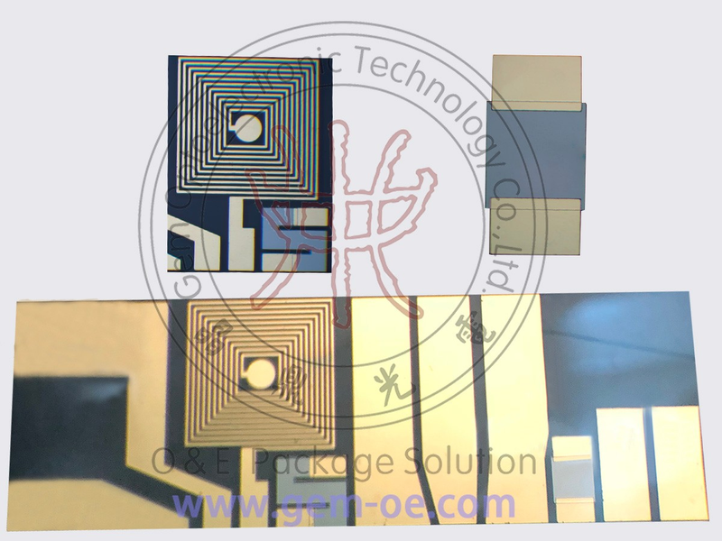
Bore film electrical resistance material: TaN、Pt、NiCr Face resistance: 10Ω/□、50Ω/□、100Ω/□ Precision Absorption: Laser offset (0.5 per cent)
1 small electrical resistance; 50 large electrical resistance; 5 per cent precision; 10 per cent special precision; 0.5 per cent precision of electrons
-
 ceramics
Ceramic and Glass Components
Gem-oe
ceramics
Ceramic and Glass Components
Gem-oe
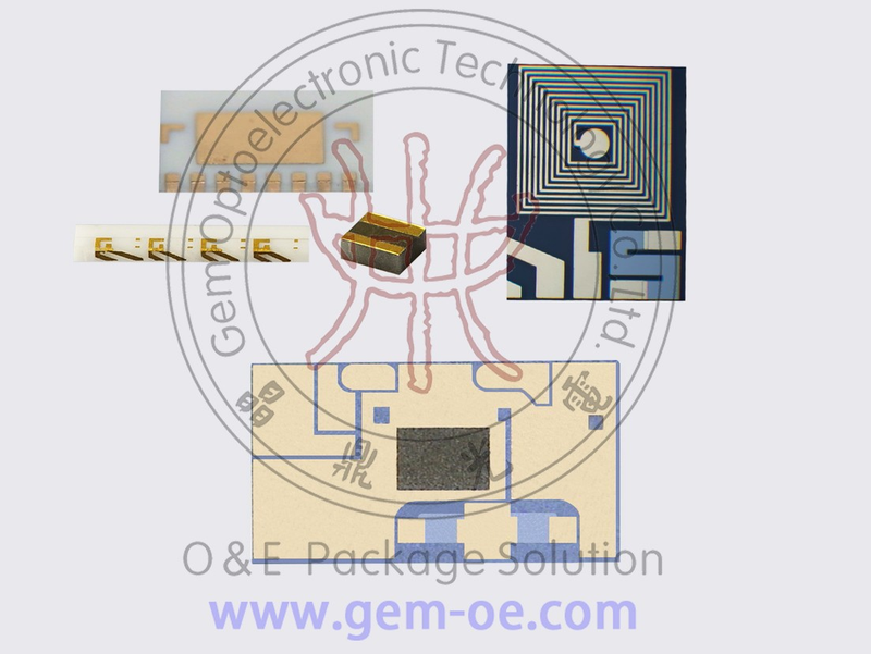
Membrane structure: Cr/Ni/Au=100~150nm/300~400nm/500~600nm, 1200~1300nm, 2800~3000nm; Ti/Pt/Au=100~150nm/200~300nm/500~600nm, 1200~1300nm, 2,800~3000nm Membrane: Ion spatter, evaporated deposition with ion aid Graphical technology: Semiconductor optical, laser etching; nano mask + photogram; lift-off
Submount, pottery thermal sunk, ceramic capacitor, thin membrane electrical resistance; metalization patterns; pottery piece products such as prefabricated gold tin; size, performance parameters, etc., can be tailored to the customer ' s needs
Related Articles
CytoViva delivers comprehensive hyperspectral imaging solutions covering visible to near-infrared spectrum, compatible with brightfield, fluorescence and proprietary enhanced darkfield microscopy modes.
Wuhan Optics Valley Quantum Technology Co., Ltd. is a leading domestic developer of high‑speed semiconductor optical chips and photodetector components. Our product portfolio covers InGaAs avalanche photodiode bare dies and PIN photodetector chips designed for fiber‑optic communication
Founded in 2019, Jilin JC Ultrafast Equipment Co., Ltd. is a high-tech enterprise incubated by the Ultrafast Optoelectronics Center of Jilin University. Our R&D team owns 15 years of profound experience in femtosecond laser micro-nano fabrication.
Driven by the continuous pursuit of higher precision and efficiency in optical communication and optoelectronic device manufacturing, OLCR-1000 Low-Coherence Interferometer, independently developed by Wuhan Guanggu Interconnect Technology Co., Ltd., provides an innovative technical solution for distributed return loss testing of optical fibers and optoelectronic devices.
Loading...
Name
Phone
Organization
Use Case

Database Platform