
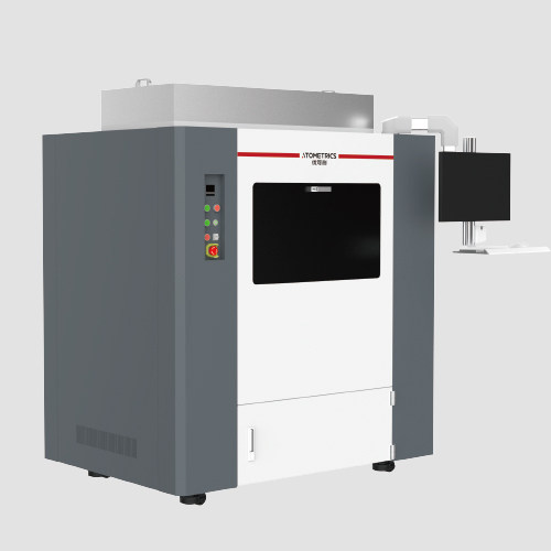
Wafer Thickness/TTV/Warpage Automatic Measurement Equipment APS Series
Suitable for overall thickness inspection of silicon wafers and compound semiconductor samples (GaAs, InP, SiC, GaN) and parameter inspection such as TTV/BOW/Warp warpage. The equipment is compatible with both transparent and opaque wafers. It uses a non-contact measurement method that is precise and fast. Using a white-light source with an upper and lower dual-probe design, the sample is placed between the two probes during testing, and one test quickly provides all information related to sample thickness and geometric parameters: thickness, TTV, Bow, Warp, TIR, LTV, etc. The equipment can also be equipped with infrared interference probes. 01 Fully automatic measurement Extremely simple operation, easy online programming settings, automatic measurement, Mapping mode supported; 02 Powerful measurement functions One test can simultaneously obtain all data: thickness, TTV, Bow, Warp, TIR, LTV, etc.; 03 Fast measurement speed Supports flying-spot sampling, quickly completing measurements and saving production time; 04 Wide application scenarios The APS series can adapt to many different products, scenarios and needs, providing you with the optimal solution
 Save to Favorites
Overview
Applications
Datasheet
Please provide your email to download the datasheet.
Invalid email format. Please try again.
Supplier Information
Related Products
-
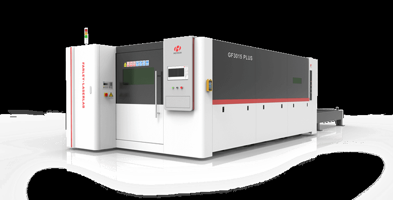 GF PLUS series dual exchange platform GF3015Plus
Semiconductor Packaging Equipment
Hglaser
GF PLUS series dual exchange platform GF3015Plus
Semiconductor Packaging Equipment
Hglaser
Machine-bed process: 1530; 3050; 250mm Contact maximum position speed: 140m/min Speed up: 1.2G
The GF PLUS series of two-way exchange platforms, using an autonomous fibre-optic laser generator; providing users with robust cutting power and efficiency; equipping specialized laser cutting control systems; gathering high stability, characterization, high power, high performance; speed faster than one; and cutting-edge machines for metal material processing!
-
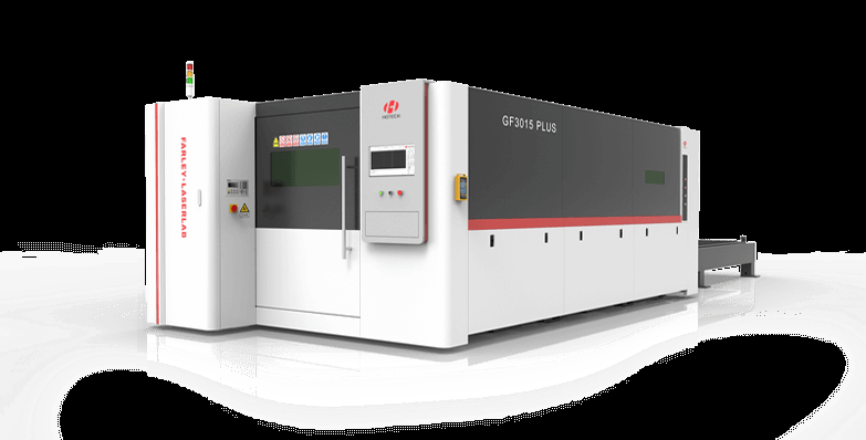 GF PLUS series dual exchange platform GF4022Plus
Semiconductor Packaging Equipment
Hglaser
GF PLUS series dual exchange platform GF4022Plus
Semiconductor Packaging Equipment
Hglaser
Machine-bed process: 2230; 4050; 250mm Contact maximum position speed: 140m/min Speed up: 1.2G
The GF PLUS series of two-way exchange platforms, using an autonomous fibre-optic laser generator; providing users with robust cutting power and efficiency; equipping specialized laser cutting control systems; gathering high stability, characterization, high power, high performance; speed faster than one; and cutting-edge machines for metal material processing!
-
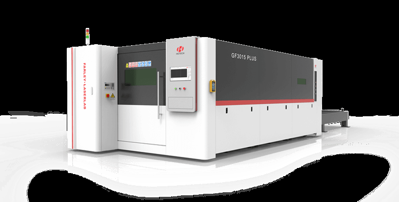 GF PLUS series dual exchange platform GF6025Plus
Semiconductor Packaging Equipment
Hglaser
GF PLUS series dual exchange platform GF6025Plus
Semiconductor Packaging Equipment
Hglaser
Machine-bed process: 2530; 6050; 250mm Contact maximum position speed: 140m/min Speed up: 1.2G
The GF PLUS series of two-way exchange platforms, using an autonomous fibre-optic laser generator; providing users with robust cutting power and efficiency; equipping specialized laser cutting control systems; gathering high stability, characterization, high power, high performance; speed faster than one; and cutting-edge machines for metal material processing!
-
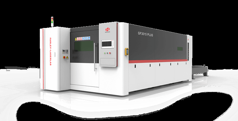 GF PLUS series dual exchange platform GF8025Plus
Semiconductor Packaging Equipment
Hglaser
GF PLUS series dual exchange platform GF8025Plus
Semiconductor Packaging Equipment
Hglaser
Machine-bed process: 2530; 8050; 250mm Contact maximum position speed: 140m/min Speed up: 1.2G
The GF PLUS series of two-way exchange platforms, using an autonomous fibre-optic laser generator; providing users with robust cutting power and efficiency; equipping specialized laser cutting control systems; gathering high stability, characterization, high power, high performance; speed faster than one; and cutting-edge machines for metal material processing!
-
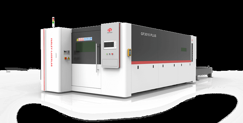 GF PLUS series dual exchange platform GF10025Plus
Semiconductor Packaging Equipment
Hglaser
GF PLUS series dual exchange platform GF10025Plus
Semiconductor Packaging Equipment
Hglaser
Machine-bed process: 2530; 10050; 250mm Contact maximum position speed: 140m/min Speed up: 1.2G
The GF PLUS series of two-way exchange platforms, using an autonomous fibre-optic laser generator; providing users with robust cutting power and efficiency; equipping specialized laser cutting control systems; gathering high stability, characterization, high power, high performance; speed faster than one; and cutting-edge machines for metal material processing!
Related Articles
As a professional manufacturer of precision optical thin-film components, sycco-optics (Shandong Yanggu Hengjing Optoelectronics) launches high-performance 850nm narrow band pass filters for near-infrared precision detection, intelligent sensing and optical imaging systems. Adopting advanced vacuum coating technology, the filter realizes high transmittance in the target band and deep blocking in interference bands. It effectively eliminates stray light and spectral noise, serving as a core optical component for machine vision, biochemical detection and photoelectric sensing equipment.
Wuhan Optics Valley Quantum Technology Co., Ltd. is a leading domestic developer of high‑speed semiconductor optical chips and photodetector components. Our product portfolio covers InGaAs avalanche photodiode bare dies and PIN photodetector chips designed for fiber‑optic communication
A microlens array (MLA) is a high-precision optical component composed of hundreds or thousands of tiny, uniformly arranged micro lenses on a single flat substrate. Unlike traditional single lenses that focus one light beam, a microlens array can split, homogenize, and reshape light on a micro scale. It is widely paired with VCSELs, lasers, and image sensors, becoming a core part of modern miniature optical systems.
Shandong Huaguang Optoelectronics Co., Ltd. (HAUCORE) is a leading high-tech manufacturer of compound semiconductor optoelectronic devices, founded in 1999 and headquartered in Jinan, China, with two R&D and production bases in Jinan and Weifang.
Loading...
Name
Phone
Organization
Use Case

Database Platform