
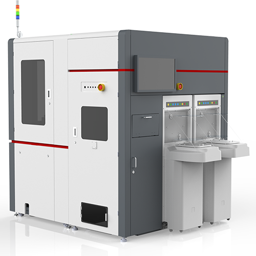
Wafer 3D Metrology Equipment WPM Series
White-light interferometry, spectral reflectance and chromatic confocal in one! Programmed measurement: intelligent arrays, automatic measurement, autofocus, automatic positioning, Data Feedback database management; High ease of use, automatic retesting, data statistical analysis with more analysis functions, one-click report generation; More functions: lean manufacturing modules such as data statistical analysis support customized development.; 01 Rich measurement functions Roughness/film thickness/step height/critical dimensions/Warpage/Bow/Stress/; 02 Ultra-high measurement accuracy Profile repeatability 0.03 nm Step height accuracy 0.3% XY maximum repeatability 0.19μm; 03 Ultra-high inspection efficiency Ultra-fast scanning speed: 5 times that of conventional models Fully automatic measurement: online programming settings, automatic measurement Offline analysis: original data can be secondarily analyzed for specific purposes
 Save to Favorites
Overview
Specifications
| Parameter | Value |
|---|---|
| Topography Repeatability | 0.03nm |
| Step Height Accuracy | 0.3% |
| XY Maximum Repeatability | 0.19μm |
Applications
Datasheet
Please provide your email to download the datasheet.
Invalid email format. Please try again.
Supplier Information
Related Products
-
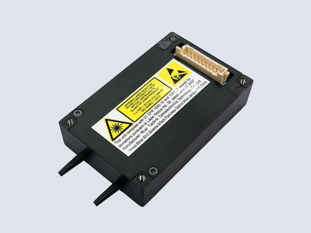 Mini EDFA Series
Semiconductor Packaging Equipment
Taclink
size: 35 mm x18 mm x5.5 mm, Smaller Output Power: >4dBm Power Consumption: <2w
Mini EDFA series, its main features are small size and low power.
-
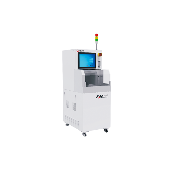 Single-axis precision dicing machine (semi-automatic)
Semiconductor Packaging Equipment
Qhlaser
Stage format: 310 mm × 310 mm X-axis working stroke: 0-600 mm Y1, Y2 axis working stroke: 0-500mm
● Wafer cutting equipment using high-precision bidirectional silent air spindle:; ● Cutting area: 4 inch, 6 inch wafers;; ● High precision: for resin substrates with irregular expansion and contraction, high-precision processing is possible through cutting line calibration at multiple points;; ● Simple and convenient operation: 17-inch touch screen;; ● Automatic blade mark calibration function: automatically measures the offset of the cutting street and the width of the cutting mark, managing processing quality;; ● Blade breakage detection function: blade breakage detection during cutting.; ● 4/6 inch IC, wafer cutting; ● Silicon, quartz, aluminum oxide, iron oxide, gallium arsenide, sapphire, glass, etc.
-
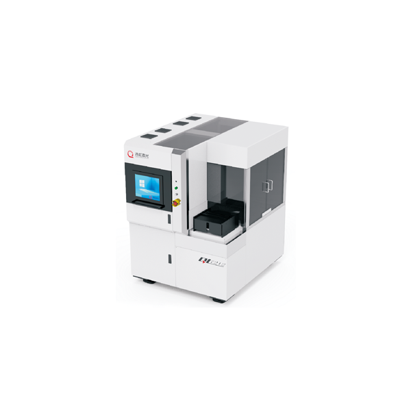 Dual-spindle precision dicing saw (fully automatic)
Semiconductor Packaging Equipment
Qhlaser
Stage format: ∅300 mm X-axis working stroke: 0-770mm Y1, Y2 axis working stroke: 0-470mm
Large-scale package substrate cutting equipment using opposed, high-precision bidirectional silent air spindles:; ● High production efficiency: basket loading, automatic loading/unloading + automatic cutting + automatic cleaning functions;; ● High precision: for resin substrates with irregular stretchable materials, high-precision processing is possible through multi-point cutting line calibration;; ● Simple and convenient operation: 19-inch touch screen;; ● Automatic calibration function: calibration can be performed by selecting recorded workpiece data;; ● Automatic blade mark calibration function: automatically measures the offset of the cutting street and the width of the cutting mark, managing processing quality;; ● More complete functions: supports diverse full-cut/half-cut processes, a more advanced ∅300mm format cutting machine.; ● Large-scale package substrates; ● IC, LED, QFN, etc.; ● Silicon, quartz, alumina, iron oxide, gallium arsenide, sapphire and glass, etc.
-
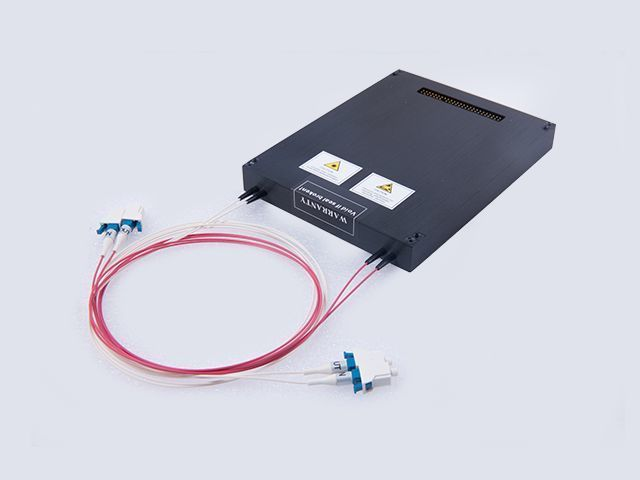 Normal EDFA Series (EDFA-BA,PA,LA)
Semiconductor Packaging Equipment
Taclink
Power: High power and High gain Gain ripple [typ. condition]: <1.0dB typ. condition NF [for typ. C Condition]: <6.0dB for typ. C Condition
Normal-type EDFA, including single-wave, multi-wave, pure optical, and powered EDFA, with dimensions above 90*70*15mm, can achieve higher gain and larger power output.
-
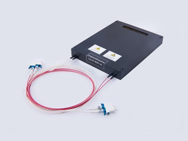 Normal EDFA Series (EDFA-VGA)
Semiconductor Packaging Equipment
Taclink
Variable Gain Range: >10dB Power: >18dBm Gain ripple [typ. condition]: <1.0dB typ. Condition
Normal-type EDFA, including single-wave, multi-wave, pure optical, and powered EDFA, with dimensions above 90*70*15mm, can achieve higher gain and larger power output.
Related Articles
Wuhan Optical Valley Interlink Technology Co., Ltd. was founded in 2013 by a technical team from Huazhong University of Science and Technology.
Shanghai Connet Laser Technology Co., Ltd. focuses on technological innovation, delivering cutting-edge photonic products & solutions for industrial lasers, LiDAR, fiber optic sensing, coherent telecom, cold atom physics and precision spectroscopy research & mass manufacturing.
Against the evolving demands for military‑grade hardware, rail transit equipment and heavy‑duty machinery that run under high‑shock vibrating conditions, anti‑loose connectors serve as indispensable hardware for stable power delivery and high‑speed signal transmission.
BEIJING JIEPU TREND supplies YAG+Er:YAG+YAG bonded composite slab laser crystals for high‑power solid‑state laser systems. The monolithic slab consists of two undoped YAG end‑cap layers and a central Er‑doped YAG gain segment. The overall dimension is 9 mm×9 mm×9 mm.
Loading...
Name
Phone
Organization
Use Case

Database Platform