


TITAN™ Multi-Contact Probe
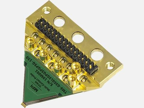
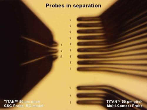
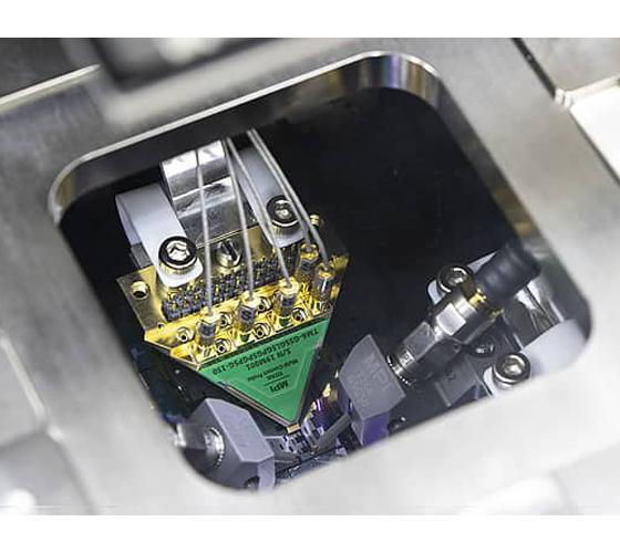
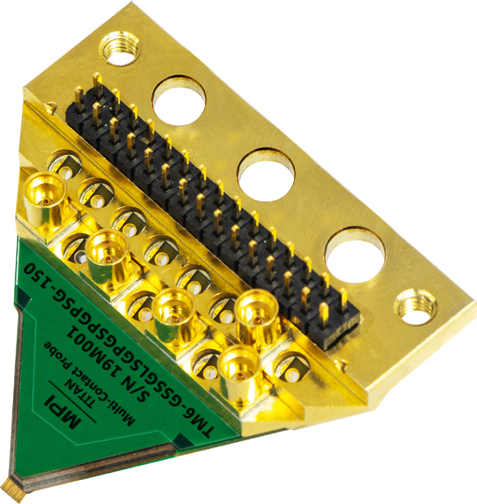
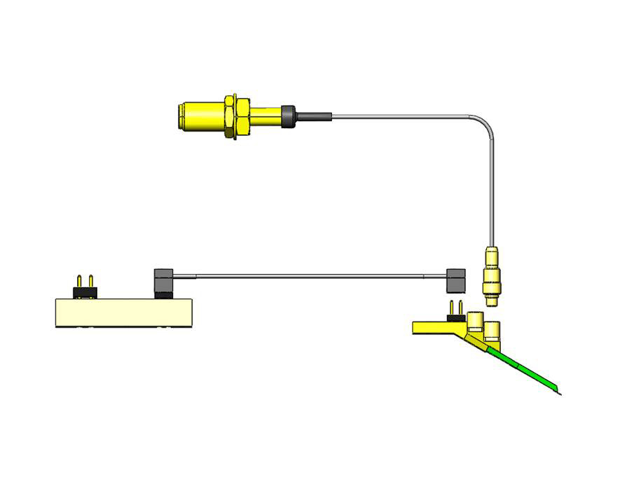
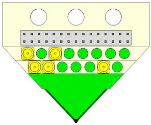
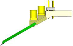
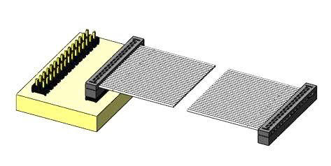
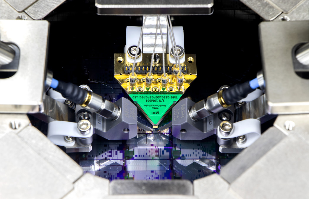
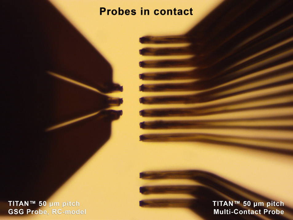
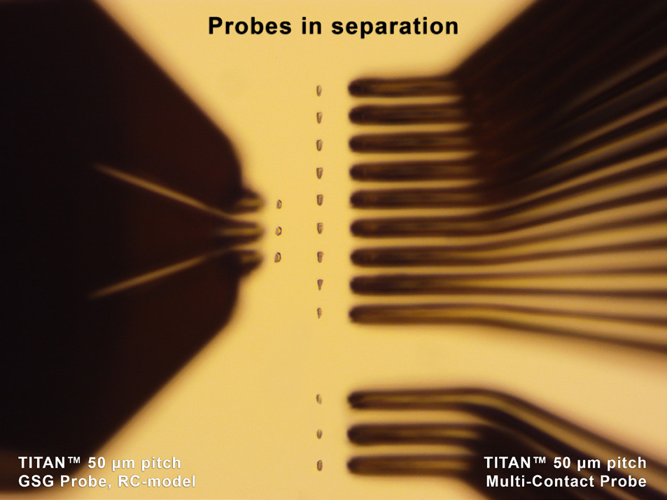
The TITAN™ Multi-Contact Probe is an advanced RF probing technology designed for the characterization of RF ICs. It features up to 15 contacts that can be individually configured for RF, logic signal, and bypass power supply. This probe offers excellent impedance matching, unique tip visibility, and a wide temperature range, making it ideal for testing high-speed digital circuits and modern multi-stage PAs.
 Save to Favorites
Overview
Specifications
| Parameter | Value |
|---|---|
| Number of contacts | 3-15 |
| Pitch | 50μm to 150μm, 25μm step; 150μm to 300μm, 50μm step |
| Temperature Range | -40 to 150°C |
| Contact width | 20μm |
| Quadrant compatible | Yes |
| ShieldEnvironment™ compatible | Yes |
| Recommended overtravel | 25μm |
| Contact Resistance | <45mΩ |
| Lifetime | >1,000,000 touchdowns |
| Types of contact | G (Ground), S (RF signal 6GHz), L (Logic signal 500MHz), P (Bypass power DC), X (No contact) |
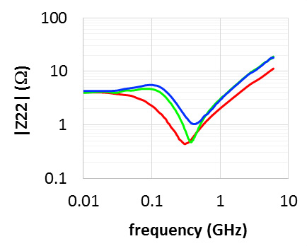
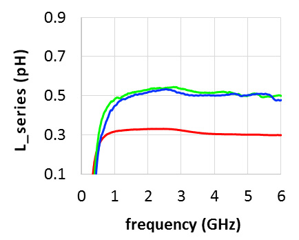
| Series Resistance | S: 0.2Ω (without cable assembly), 0.7Ω (with cable assembly); L: 0.2Ω (without cable assembly), 0.4Ω (with cable assembly); P: 0.2Ω (without cable assembly), 0.4Ω (with cable assembly) |
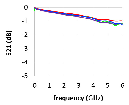
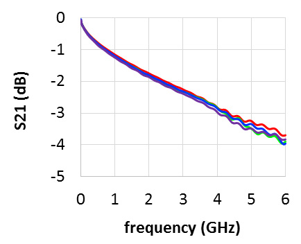
| Standard RF Insertion Loss | 3dB (without cable assembly), 5dB (with cable assembly) |
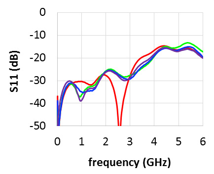
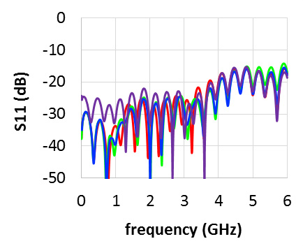
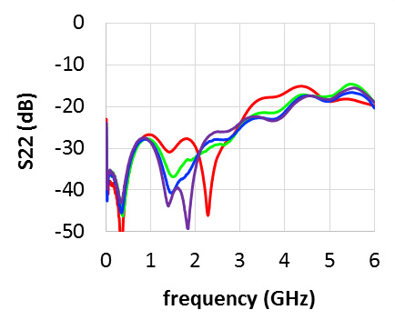
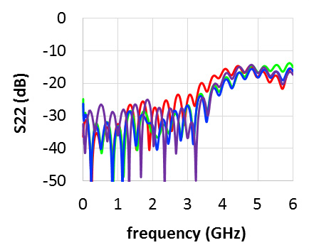
| Standard RF Return Loss | 10dB |
| Bandwidth for Logic & Nonstandard RF | L (any): 500MHz (without cable assembly), 70MHz (with cable assembly); S without adjacent G: 500MHz |
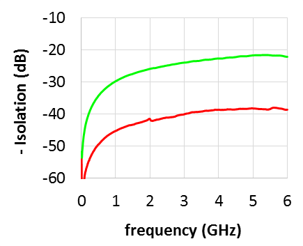
| Isolation | SGS: 20dB (50μm to 150μm pitch), 25dB (200μm to 300μm pitch); SS: 15dB |
| Bypass Power | GPG, G+P+G: 6Ω, 0.4nH; GP, G+P: 7Ω, 0.7nH |
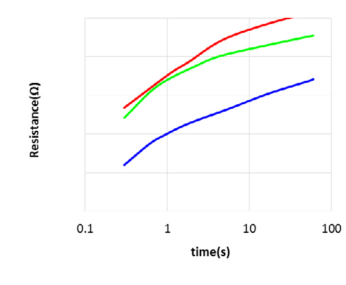
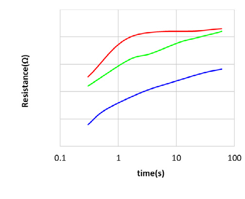
| Open Resistance Between Adjacent Lines | Standard Edition: S-G: 100MΩ, S-S: 100MΩ, L-G: 100MΩ, L-L: 100MΩ, P-G: 100MΩ, P-P: 100MΩ; Low Leakage Premium Edition: S-G: 20GΩ (0.3s-3s), 100GΩ (after 30s); S-S: 20GΩ (0.3s-3s), 100GΩ (after 30s); L-G: 20GΩ (0.3s-3s), 200GΩ (after 30s); L-L: 20GΩ (0.3s-3s), 200GΩ (after 30s); P-G: 1GΩ (0.3s-3s), 15GΩ (after 30s); P-P: 1GΩ (0.3s-3s), 100GΩ (after 30s) |
| Dimensions | 39.9mm×28.7mm×6.0mm |
| Recommended IC Pad Size | Minimum width and length vary based on pitch and number of contacts, ranging from 25μm×20μm to 70μm×40μm |
Applications
Key Features
Datasheet
Supplier Information
Related Products
-
 Unknown
Probe Station Accessories
Yokogawa
Unknown
Probe Station Accessories
Yokogawa
Cable Length: Unknown Connector Type: Unknown Material: Unknown
This product appears to be a specialized optical device, likely used for precision applications in the photonics industry.
-
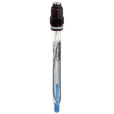 Type 8203 pH and ORP Probes
Probe Station Accessories
Burkert
Type 8203 pH and ORP Probes
Probe Station Accessories
Burkert
Measuring Range (mV): -2000...+2000 Fluid Temperature (°C): -10...+140
Type 8203 probes are designed for measuring pH or ORP in clean or contaminated liquids, including those with sulfides, proteins, or low conductivity.
-
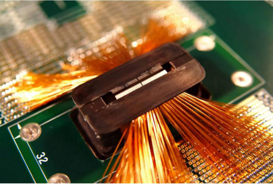 Unknown
Probe Station Accessories
Ybsemi-Solution
Unknown
Probe Station Accessories
Ybsemi-Solution
Number of Wires: Multiple Connection Type: High-density Operating Temperature: -40°C to +85°C
This product is a high-performance optical component designed for advanced electronic and photonic applications.
-
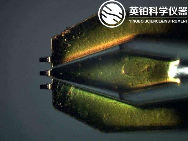 TITAN™ Probe Family DC to 145 GHz
Probe Station Accessories
Ybsemi-Solution
TITAN™ Probe Family DC to 145 GHz
Probe Station Accessories
Ybsemi-Solution
Characteristic Impedance: 50Ω Connector Type: 0.8mm, female Tip Material: Ni alloy
The TITAN™ Probe Family offers unparalleled accuracy for single-ended and differential calibration, device, and circuit characterization across a wide frequency range up to 145 GHz.
-
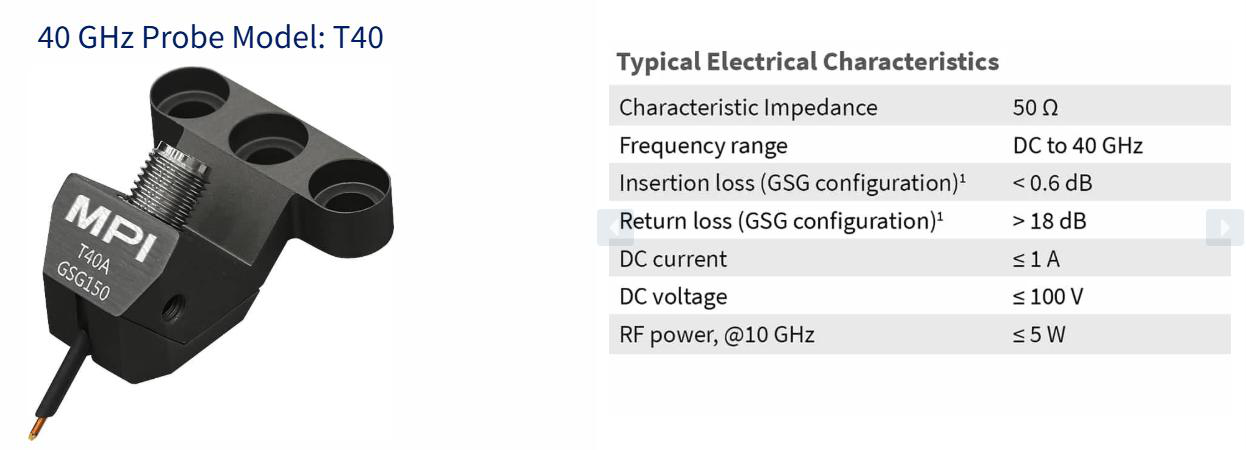 TITAN™ Probe Series
Probe Station Accessories
Ybsemi-Solution
TITAN™ Probe Series
Probe Station Accessories
Ybsemi-Solution
Characteristic Impedance: 50Ω Frequency Range: DC to 220GHz Insertion Loss (dB): <5
The TITAN™ Probe Series offers advanced RF probes designed for high-frequency and high-power applications. These probes are equipped with MEMS contact tips, ensuring unmatched calibration accuracy and reliability across a wide frequency range. They are ideal for RF testing, mmWave devices, and S-parameter measurements.
Related Articles
Shanghai Connet Laser Technology Co., Ltd. focuses on technological innovation, delivering cutting-edge photonic products & solutions for industrial lasers, LiDAR, fiber optic sensing, coherent telecom, cold atom physics and precision spectroscopy research & mass manufacturing.
A solid-state laser is one of the most common and reliable laser types used in modern industry, medical equipment, and scientific research. Unlike gas or fiber lasers, it uses solid materials as its gain medium to generate stable, high-brightness laser beams. Thanks to its high precision, long lifespan, and compact structure, solid-state lasers have become a mainstream solution for high-precision laser processing and optical systems.
Looking for a market-verified 808nm pump laser diode? This guide introduces HAUCORE DM-8E5A-8OD (HGLD-808-COS-D-5W), its core advantages, key specs and mainstream industrial, medical & research applications.
Founded in 2003, BWT Beijing Optoelectronics adheres to the mission "Let Dreams Fly With Light" and vision of becoming a Global Leader in Laser Solutions, guided by the core value "Innovate to Achieve Extraordinary".
Loading...
Name
Phone
Organization
Use Case

Database Platform