
Laser Cutting
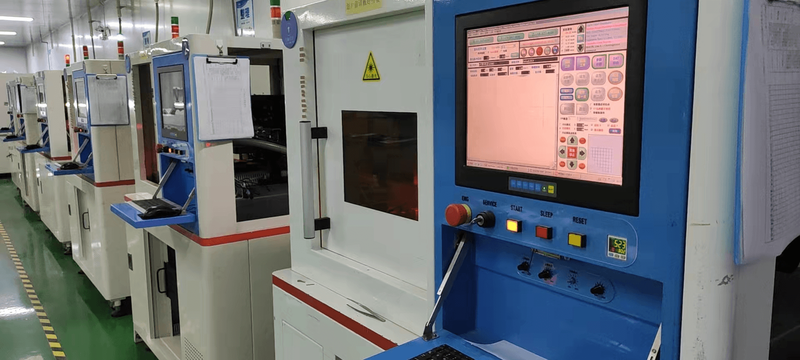
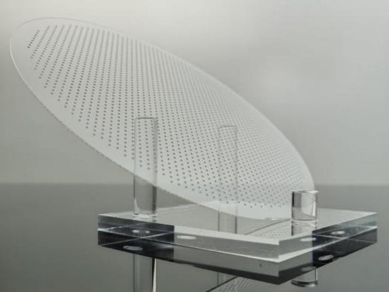
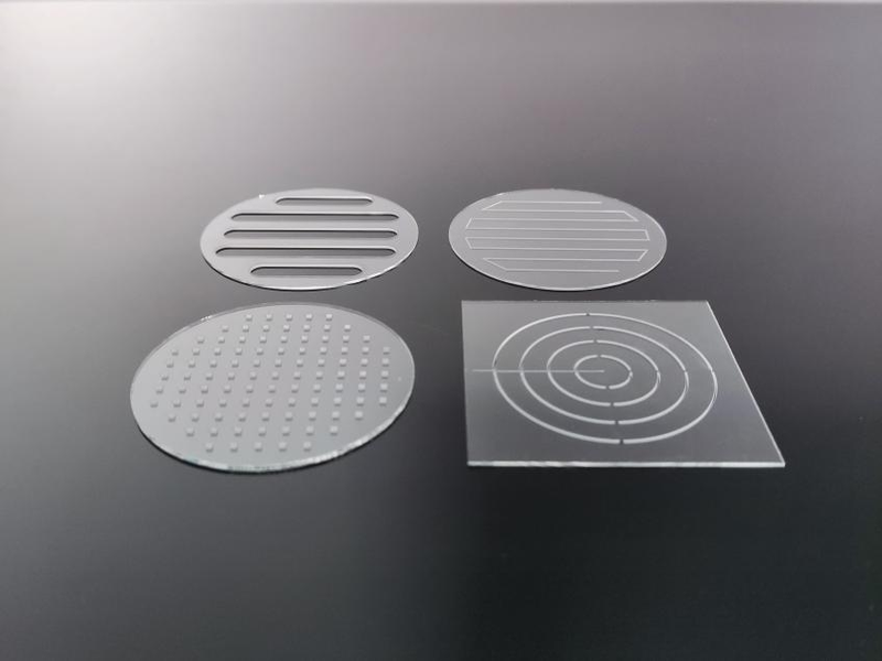
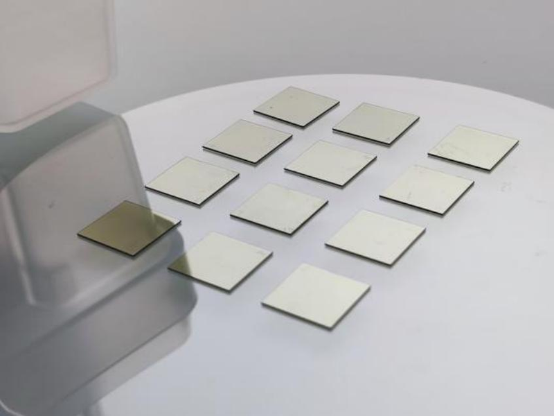
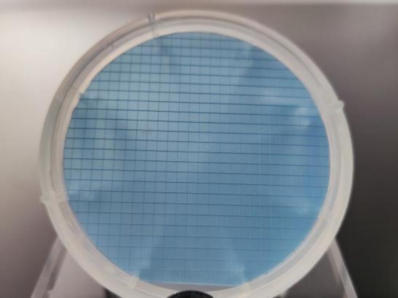
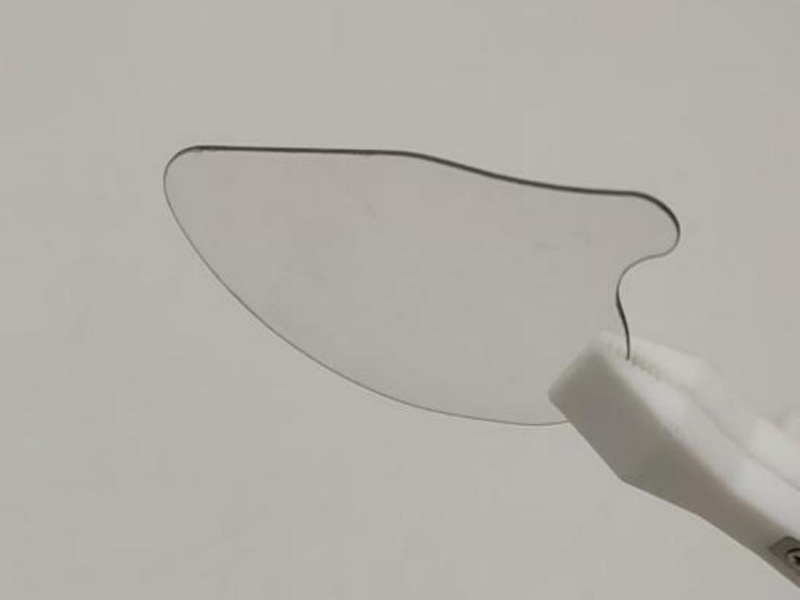
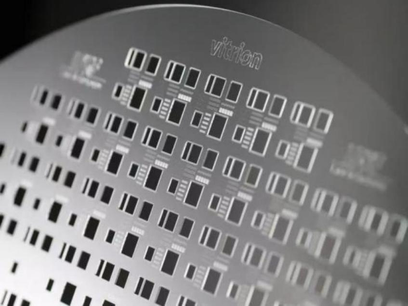
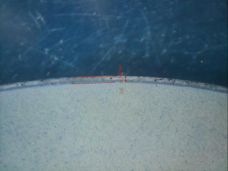
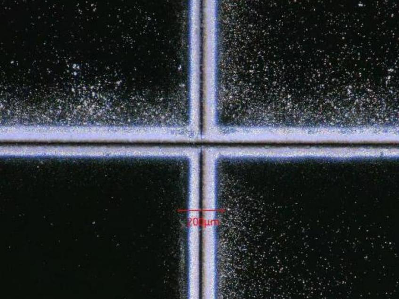
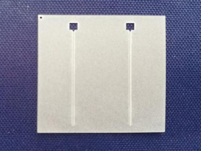
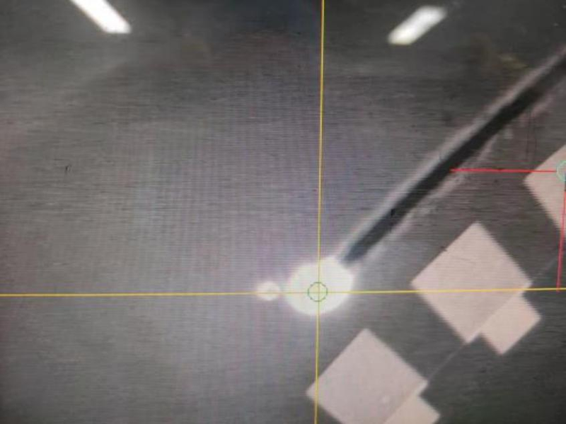
Laser cutting is a precise, noncontact process widely used in advanced wafer-semiconductor manufacturing. A focused high-energy beam locally melts or vaporizes material through photothermal effects. Wavelength, power and pulse width are adjusted to material properties for optimal cuts. 晶沐光电 has its own laser-processing line with UV/ultrafast lasers, wafer infrared stealth-dicing and cleaving machines, infrared fiber cutting machines and other equipment for varied wafer-cutting needs.
 Save to Favorites
Overview
Applications
Key Features
Datasheet
Please provide your email to download the datasheet.
Invalid email format. Please try again.
Supplier Information
Related Products
-
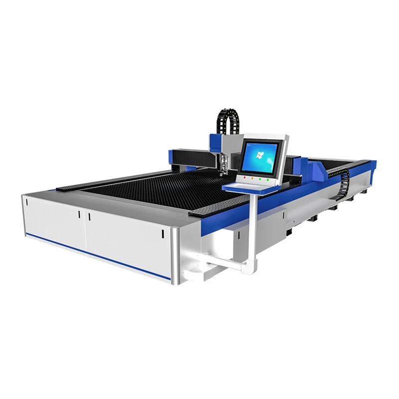 Open Single Table Sheet Laser Cutting Machine BLS3015
Laser Processing Equipment
Auroralaser
Working Area: 3000*1500 Table Load Bearing: 2000 kg Overall Dimensions: 4850 mm × 2330 mm × 1920 mm
BLS Series Open Single Table Sheet Laser Cutting Machine The “single table” and “open-frame” design are ideal solutions for sheet metal processing scenarios that prioritize cost-effectiveness, operational convenience, and flexible adaptability.
-
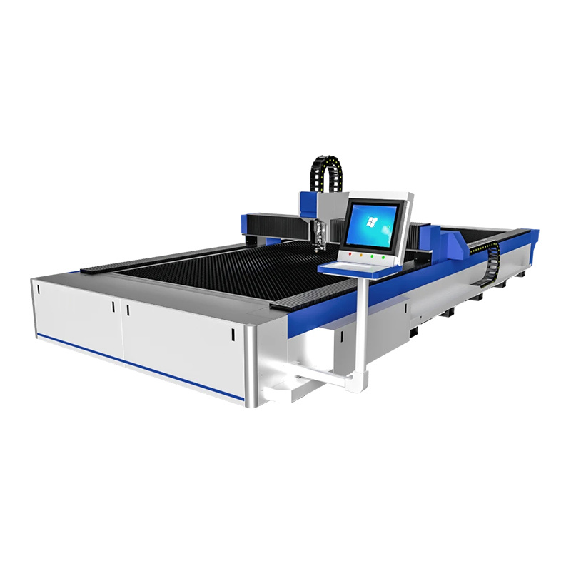 Open Single Table Sheet Laser Cutting Machine BLS4015
Laser Processing Equipment
Auroralaser
Working Area: 4000*1500 Table Load Bearing: 2500 kg Overall Dimensions: 5850 mm × 2330 mm × 1920 mm
BLS Series Open Single Table Sheet Laser Cutting Machine The “single table” and “open-frame” design are ideal solutions for sheet metal processing scenarios that prioritize cost-effectiveness, operational convenience, and flexible adaptability.
-
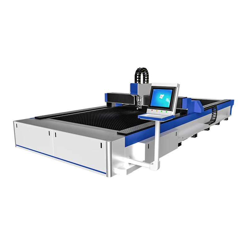 Open Single Table Sheet Laser Cutting Machine BLS6015
Laser Processing Equipment
Auroralaser
Working Area: 6000*1500 Table Load Bearing: 3500 kg Overall Dimensions: 7920 mm × 2330 mm × 1920 mm
BLS Series Open Single Table Sheet Laser Cutting Machine The “single table” and “open-frame” design are ideal solutions for sheet metal processing scenarios that prioritize cost-effectiveness, operational convenience, and flexible adaptability.
-
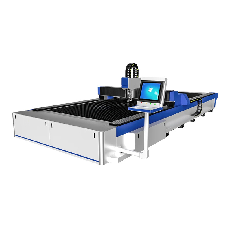 Open Single Table Sheet Laser Cutting Machine BLS6020
Laser Processing Equipment
Auroralaser
Working Area: 6000*2000 Table Load Bearing: 5000 kg Overall Dimensions: 7920 mm × 2880 mm × 1920 mm
BLS Series Open Single Table Sheet Laser Cutting Machine The “single table” and “open-frame” design are ideal solutions for sheet metal processing scenarios that prioritize cost-effectiveness, operational convenience, and flexible adaptability.
Related Articles
Founded in 2019, Jilin JC Ultrafast Equipment Co., Ltd. is a high-tech enterprise incubated by the Ultrafast Optoelectronics Center of Jilin University. Our R&D team owns 15 years of profound experience in femtosecond laser micro-nano fabrication.
VCSEL, short for Vertical Cavity Surface Emitting Laser, is a widely used semiconductor laser component in modern optoelectronics. Unlike traditional edge-emitting lasers, VCSEL emits laser light vertically from its chip surface. Thanks to its low power consumption, stable beam quality, low cost, and easy integration, it has become the core light source for 3D sensing, wearable devices, and high-speed optical communication.
Driven by the rapid upgrading of intelligent vehicles, optoelectronic sensing technologies represented by laser sensing and infrared thermal imaging have become core pillars for high-level autonomous driving and smart cockpit iteration. Leveraging automotive-grade optoelectronic R&D advantages, Pilot Technology Group launches the VITAL intelligent vehicle solution. By integrating high-power VCSEL laser chips and vehicle infrared night-vision thermal imagers, the system comprehensively enhances vehicle environmental perception and realizes safer, smarter and more comfortable driving experiences.
The MSL‑T series water‑cooled continuous‑wave single‑longitudinal‑mode lasers from Changchun New Industries Optoelectronics (CNI) deliver key research wavelengths including 369 nm, 405 nm and 770 nm.
Loading...
Name
Phone
Organization
Use Case

Database Platform