
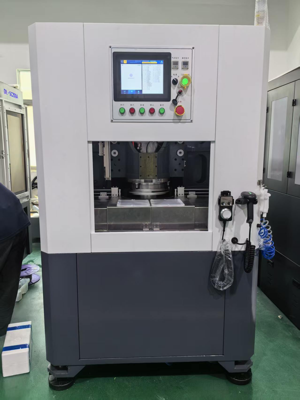
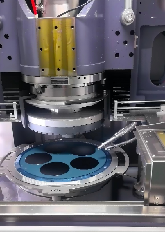
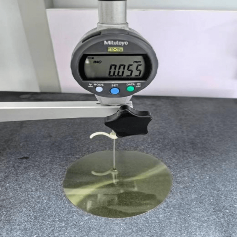
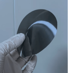
Grinding, Polishing and Thinning
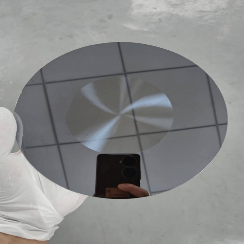
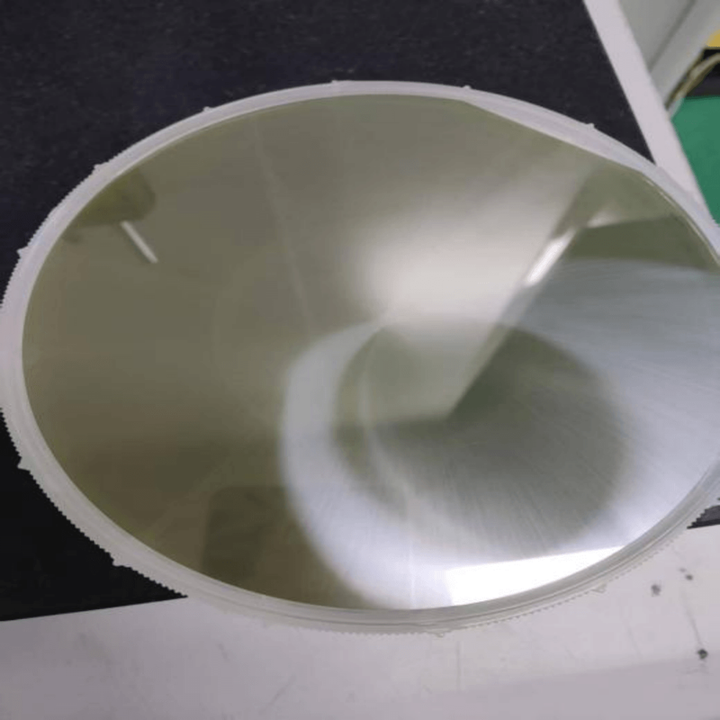
One-Stop Wafer Grinding/Thinning through Mirror Polishing,Ultrathin Thickness Control,Nanometre Flatness/Low-Damage Surfaces for Advanced Chips,Power/RF Devices,Packaging.
 Save to Favorites
Overview
Applications
Key Features
Datasheet
Please provide your email to download the datasheet.
Invalid email format. Please try again.
Supplier Information
Related Products
-
 Case Collection - 05
Custom and Other Services
Situoli
Custom Cases:Brightfield Flow-Cell Imaging,Olympus Heated Slide Holder,Fiber Centering Device,Olympus Fluorescence Cube.
-
 Case Collection - 03
Custom and Other Services
Situoli
Custom Cases:Live-Cell Environment Simulator,Olympus CX23 Binocular-to-Tube-Lens Imaging Conversion,Nikon TS2R Added IR Laser.
-
 Case Collection - 04
Custom and Other Services
Situoli
Custom Cases:Motorized Fluorescence Test Platform,Olympus CKX41 Halogen-to-LED Conversion,Olympus SZX7 Added UV Source.
-
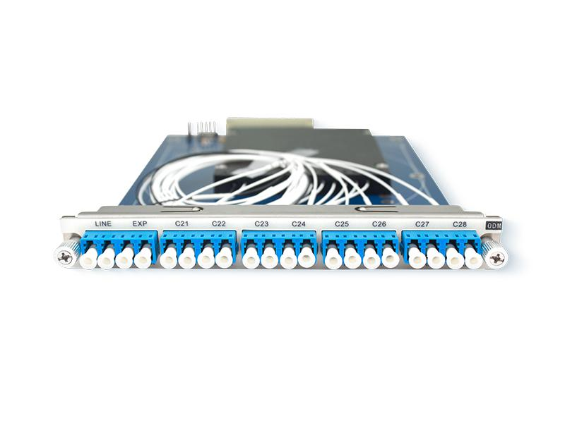 Multiplexing / Demultiplexing Board (ODM)
Custom and Other Services
Fiberwdm
Wavelength Range: CWDM:1271~1611nm DWDM:C-Band(100GHZ/75GHZ/50GHZ) Channel Spacing: CWDM:20nm DWDM:0.8nm/0.6nm/0.4nm Passband Width: CWDM:±6.5nm DWDM:0.1nm
The ODM multiplexer/demultiplexer board from FIBERWDM瑞东科技 combines or separates CWDM/DWDM channels, saving fiber resources and enabling flexible network configuration. DWDM systems smoothly upgrade to48 wavelengths at100GHz spacing,64 at75GHz and96 at50GHz. CWDM supports upgrades to18 wavelengths. Higher spectral utilization saves frequency-band resources.
Related Articles
Founded in 2019, Jilin JC Ultrafast Equipment Co., Ltd. is a high-tech enterprise incubated by the Ultrafast Optoelectronics Center of Jilin University. Our R&D team owns 15 years of profound experience in femtosecond laser micro-nano fabrication.
VCSEL, short for Vertical Cavity Surface Emitting Laser, is a widely used semiconductor laser component in modern optoelectronics. Unlike traditional edge-emitting lasers, VCSEL emits laser light vertically from its chip surface. Thanks to its low power consumption, stable beam quality, low cost, and easy integration, it has become the core light source for 3D sensing, wearable devices, and high-speed optical communication.
Driven by the rapid upgrading of intelligent vehicles, optoelectronic sensing technologies represented by laser sensing and infrared thermal imaging have become core pillars for high-level autonomous driving and smart cockpit iteration. Leveraging automotive-grade optoelectronic R&D advantages, Pilot Technology Group launches the VITAL intelligent vehicle solution. By integrating high-power VCSEL laser chips and vehicle infrared night-vision thermal imagers, the system comprehensively enhances vehicle environmental perception and realizes safer, smarter and more comfortable driving experiences.
The MSL‑T series water‑cooled continuous‑wave single‑longitudinal‑mode lasers from Changchun New Industries Optoelectronics (CNI) deliver key research wavelengths including 369 nm, 405 nm and 770 nm.
Loading...
Name
Phone
Organization
Use Case

Database Platform