
NDT4562
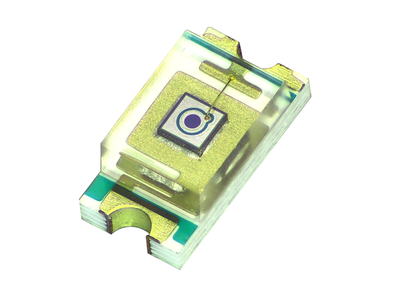
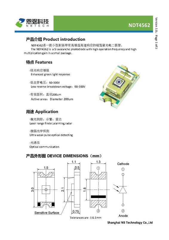
NDT4562 is a silicon avalanche photodiode in a small package, offering high gain, fast response, high operating frequency and high multiplication gain.
 Save to Favorites
Overview
Specifications
| Parameter | Value |
|---|---|
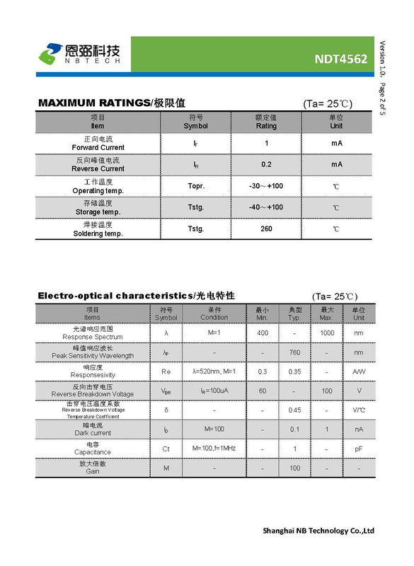
| Forward Current I_F [MAXIMUM RATINGS;Ta=25°C] | 1 mA |
| Peak Reverse Current I_R [MAXIMUM RATINGS;Ta=25°C] | 0.2 mA |
| Operating Temperature Topr. [MAXIMUM RATINGS;Ta=25°C] | -30~+100 °C |
| Storage Temperature Tstg. [MAXIMUM RATINGS;Ta=25°C] | -40~+100 °C |
| Soldering Temperature Tstg. [MAXIMUM RATINGS; Ta=25°C; Source Symbol Is Tstg., the Same as Storage Temperature; Retained as in Source] | 260 °C |
| Spectral Response Range λ [Electro-optical characteristics;Ta=25°C;M=1] | min:400 nm; max:1000 nm |
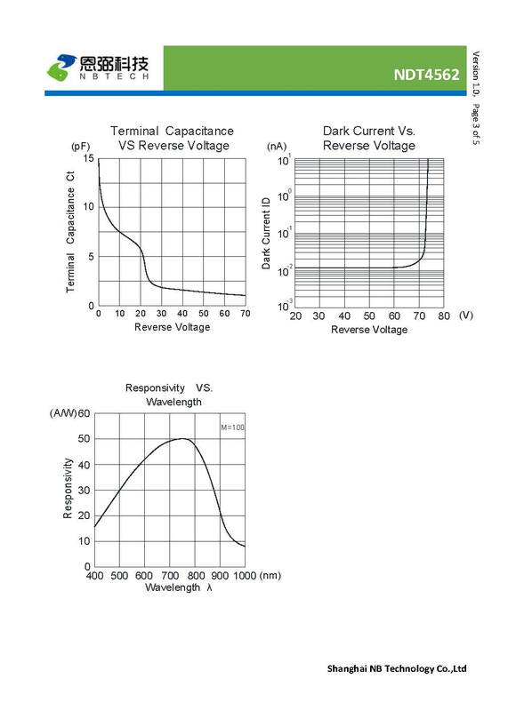
| Peak Response Wavelength λ_P [Electro-optical characteristics;Ta=25°C] | typical:760 nm |
| Responsivity Re [Electro-optical characteristics;Ta=25°C;λ=520nm;M=1] | min:0.3 A/W; typical:0.35 A/W |
| Reverse Breakdown Voltage V_BR [Electro-optical characteristics;Ta=25°C;I_R=100μA] | min:60 V; max:100 V |
| Breakdown-Voltage Temperature Coefficient δ [Electro-optical characteristics;Ta=25°C] | typical:0.45 V/°C |
| Dark Current I_D [Electro-optical characteristics;Ta=25°C;M=100] | typical:0.1 nA; max:1 nA |
| Capacitance Ct [Electro-optical characteristics;Ta=25°C;M=100;f=1MHz] | typical:1 pF |
| Amplification Factor M [Electro-optical characteristics;Ta=25°C] | Typ:100 |
| Active Area Diameter [Independent Features / Name-Value Table on PDF Page 1] | 200 μm |
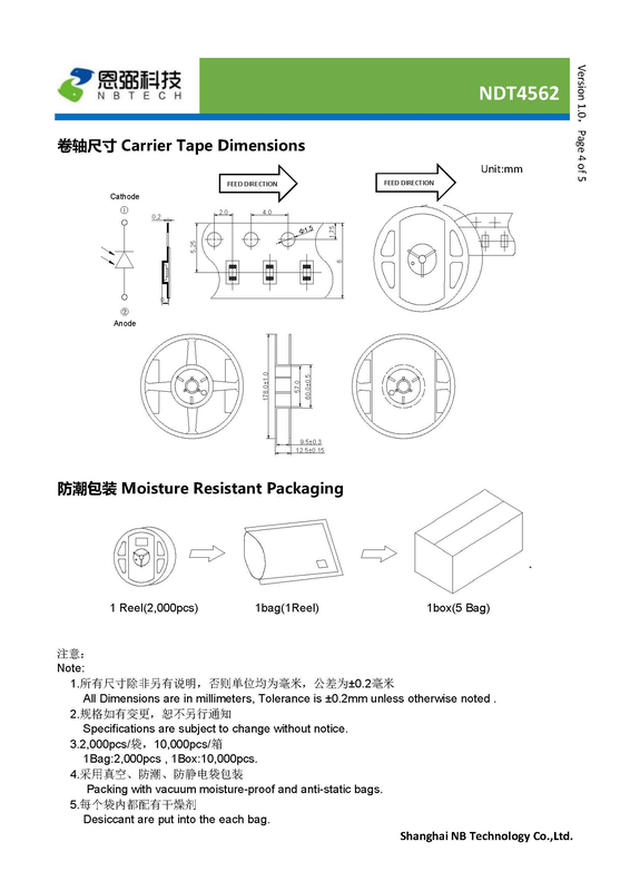
| Quantity per Package [Independent Note on PDF Page 4] | 2000pcs/Bag; 10000pcs/Box |
| Packaging Method [Independent Note on PDF Page 4] | Vacuum, Moisture-Proof, Antistatic Bag; Desiccant in Each Bag |
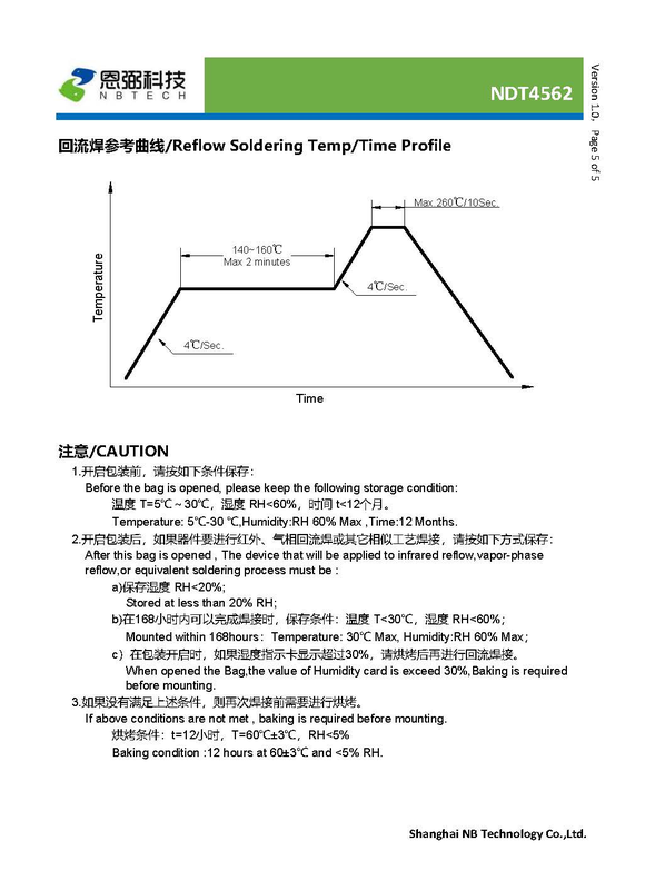
| Storage Temperature [Before Opening the Bag; Independent CAUTION on Page 5] | 5~30 °C |
| Storage Humidity [Before Opening the Bag; Independent CAUTION on Page 5, Chinese/English Boundaries Retained] | Chinese: RH<60%; English: RH60%Max |
| Storage Time [Before Opening the Bag; Independent CAUTION on Page 5] | Chinese: t<12 Months; English: Time: 12 Months |
| Storage Humidity [After Opening the Bag; For Infrared / Vapor-Phase Reflow Soldering or Similar Processes] | <20 %RH |
| Storage Temperature [Complete Soldering within 168 Hours after Opening the Bag; Independent CAUTION on Page 5] | Chinese: T<30°C; English: Temperature: 30°C Max |
| Storage Humidity [Complete Soldering within 168 Hours after Opening the Bag; Independent CAUTION on Page 5] | Chinese: RH<60%; English: RH60%Max |
| Baking Conditions [If Storage Conditions Were Not Met, Before Resoldering; Baking Also Required When the Humidity Indicator Card Shows >30% after Opening the Bag] | t=12 Hours; T=60°C±3°C; RH<5% |
Applications
Key Features
Datasheet
Supplier Information
Related Products
-
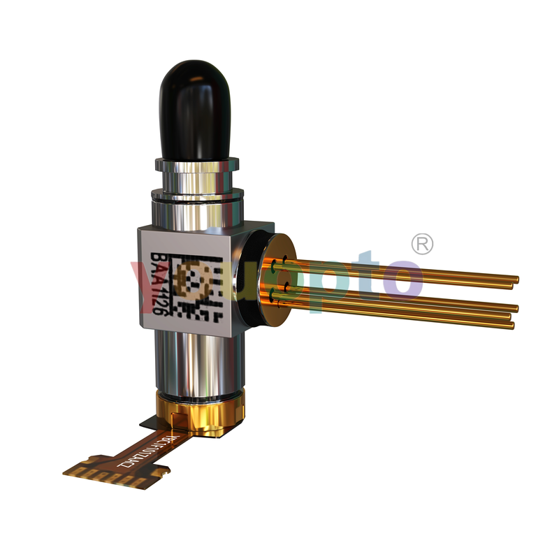 10G ZR BIDI T49R55/T55R49
Photodiodes
Youopto
Housing Operating Temperature: -5°C~+75°C
Youopto10G80km BIDI,High-Speed EML/Mini TEC/Thermistor/Monitor PD in7PIN TO56 Coax/Coax APD Receiver,Small Pluggable Telecom/Data-Center Modules.
-
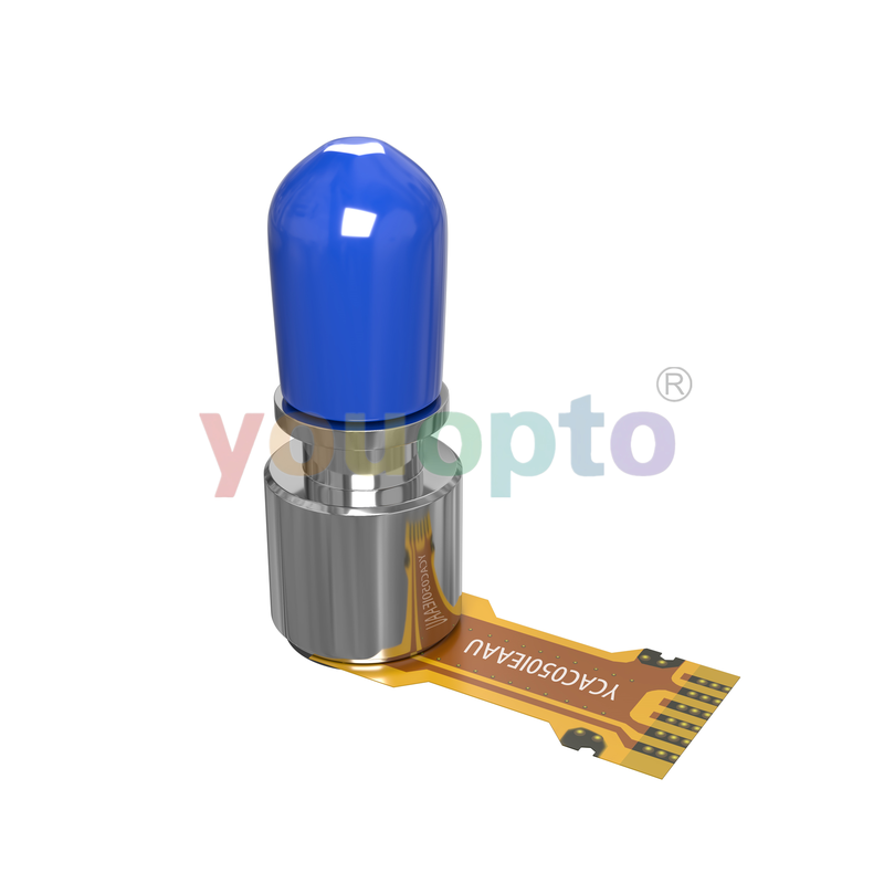 50G APD ROSA
Photodiodes
Youopto
Case Operating Temperature [Basic Range]: -5℃ to +75℃ Case Operating Temperature [Extendable Range]: -40℃ to +85℃
Youopto50G APD ROSA50Gbps,High-Speed APD/Linear TIA in7pin TO46 Coax,for Small Pluggable Telecom/Data Transceivers/Modules.
-
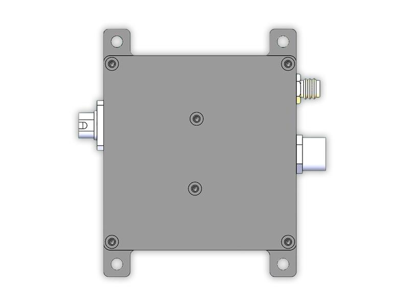 APD1050H Avalanche Detector
Photodiodes
Fiberwdm
Wavelength Range: 900-1700nm 3dB Bandwidth: DC-500MHz Conversion Gain [High-Impedance Output Load; Gain Drops to Half the Nominal Value with a 50Ω Load]: 100x10³V/A
This APD avalanche-photodetector series operates essentially like Thorlabs/Newport detectors and uses identical power connectors. It is stated to directly replace equal-bandwidth models when a Monitor output, present on some Thorlabs/Newport products, is unnecessary, with comparable or better performance. 广州瑞东's APD detectors are fully domestically produced. Proprietary temperature compensation gives high sensitivity, stability/gain and low noise across -40°C to 80°C. Standard models and customization of supply voltage, gain, bandwidth and other specifications are available. Uses include lidar, free-space optical communications, fiber sensing and optical inspection.
-
 APD1008 Avalanche Detector
Photodiodes
Fiberwdm
Wavelength Range: 900-1700nm 3dB Bandwidth: DC / AC - 80MHz Conversion Gain [High-Impedance Output Load; Gain Drops to Half the Nominal Value with a 50Ω Load]: 600 V/A × 103 V/A
广州瑞东's APD avalanche photodetector is fully domestically produced. An exclusive temperature-compensation approach provides high sensitivity, high stability, high gain and low noise throughout -40 to 80°C. In addition to standard detectors, customization can adjust supply voltage, gain, bandwidth and other parameters to customer requirements. Applications include LiDAR, free-space optical communication, fiber-optic sensing and optical inspection systems.
-
 APD2008 Avalanche Detector
Photodiodes
Fiberwdm
Wavelength Range: 400-1100nm dB Bandwidth: DC/AC-50MHz Conversion Gain [High-Impedance Output Load; Gain Drops to Half the Nominal Value with a 50Ω Load]: 3000 V/A × 103 V/A
广州瑞东's APD avalanche photodetector is fully domestically produced. An exclusive temperature-compensation approach provides high sensitivity, high stability, high gain and low noise throughout -40 to 80°C. In addition to standard detectors, customization can adjust supply voltage, gain, bandwidth and other parameters to customer requirements. Applications include LiDAR, free-space optical communication, fiber-optic sensing and optical inspection systems.
Related Articles
Founded in 2019, Jilin JC Ultrafast Equipment Co., Ltd. is a high-tech enterprise incubated by the Ultrafast Optoelectronics Center of Jilin University. Our R&D team owns 15 years of profound experience in femtosecond laser micro-nano fabrication.
VCSEL, short for Vertical Cavity Surface Emitting Laser, is a widely used semiconductor laser component in modern optoelectronics. Unlike traditional edge-emitting lasers, VCSEL emits laser light vertically from its chip surface. Thanks to its low power consumption, stable beam quality, low cost, and easy integration, it has become the core light source for 3D sensing, wearable devices, and high-speed optical communication.
Driven by the rapid upgrading of intelligent vehicles, optoelectronic sensing technologies represented by laser sensing and infrared thermal imaging have become core pillars for high-level autonomous driving and smart cockpit iteration. Leveraging automotive-grade optoelectronic R&D advantages, Pilot Technology Group launches the VITAL intelligent vehicle solution. By integrating high-power VCSEL laser chips and vehicle infrared night-vision thermal imagers, the system comprehensively enhances vehicle environmental perception and realizes safer, smarter and more comfortable driving experiences.
The MSL‑T series water‑cooled continuous‑wave single‑longitudinal‑mode lasers from Changchun New Industries Optoelectronics (CNI) deliver key research wavelengths including 369 nm, 405 nm and 770 nm.
Loading...
Name
Phone
Organization
Use Case

Database Platform