
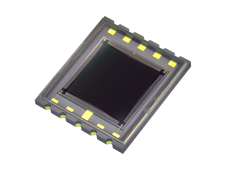
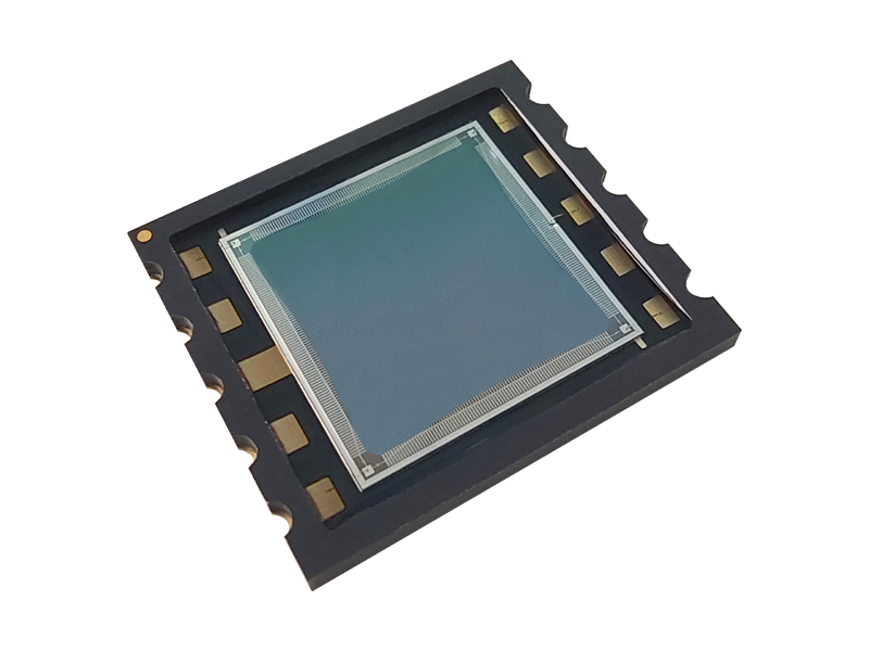
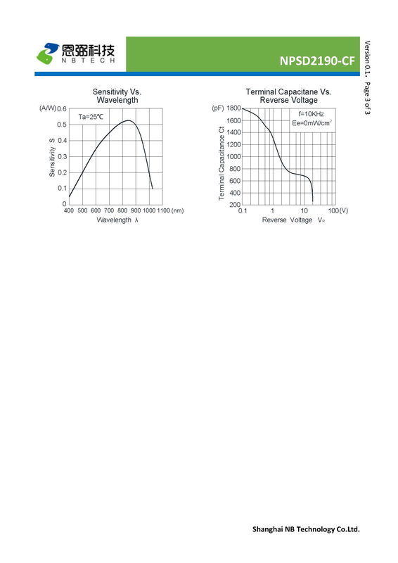
NPSD2190-CF (Two-Dimensional PSD)
NPSD2190 Surface-Mount PD,Special Structure Measures Spot-Centroid XY,High Sensitivity/Linearity/Consistency,9×9mm Active;NPSD2190-CF Ceramic+Glass,NPSD2190 Ceramic+Coating.
 Save to Favorites
Overview
Specifications
| Parameter | Value |
|---|---|
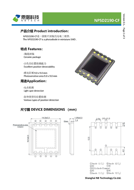
| Photosensitive Region [Reference; Independent Features on Page 1] | 9.0 mm × 9.0 mm |
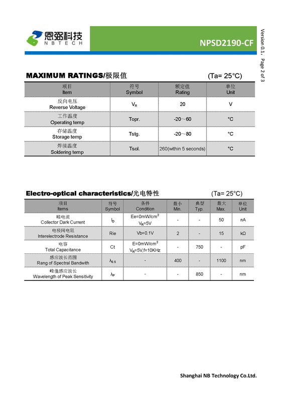
| Reverse Voltage V_R [Reference;MAXIMUM RATINGS;Ta=25°C] | 20 V |
| Operating Temperature Topr. [Reference;MAXIMUM RATINGS;Ta=25°C] | -20~60 °C |
| Storage Temperature Tstg. [Reference;MAXIMUM RATINGS;Ta=25°C] | -20~80 °C |
| Soldering Temperature Tsol. [Reference;MAXIMUM RATINGS;Ta=25°C] | 260(within 5 seconds) |
| Dark Current I_D [Reference;Electro-optical characteristics;Ta=25°C;Ee=0mW/cm²;V_R=5V] | max:50 nA |
| Interelectrode Resistance Rie [Reference;Electro-optical characteristics;Ta=25°C;Vb=0.1V] | min:2 kΩ; max:15 kΩ |
| Capacitance Ct [Reference;Electro-optical characteristics;Ta=25°C;E=0mW/cm²;V_R=5V;f=10KHz] | typical:750 pF |
| Sensing Wavelength Range λ_0.5 [Reference;Electro-optical characteristics;Ta=25°C] | min:400 nm; max:1100 nm |
| Peak Sensing Wavelength λ_P [Reference;Electro-optical characteristics;Ta=25°C] | typical:850 nm |
Applications
Key Features
Datasheet
Supplier Information
Related Products
-
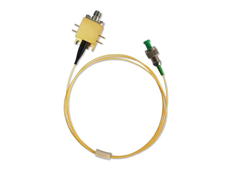 40G High-Speed Indium Gallium Arsenide (InGaAs) Photodetector HSPD4040
Optical Detectors
Fiberwdm
Storage Temperature Range TSTG [Typical Values and Absolute Maximum Ratings]: typical:-45~+85; Rated: -55~+85 Operating Case-Temperature Range TC [Typical Values and Absolute Maximum Ratings]: typical:25; Rated: -40~+85 Bias Voltage VR [Typical Values and Absolute Maximum Ratings]: typical:5; Rated: 5~6
HSPD4040 is a high-speed detector module for digital/analog applications. An InGaAs PIN photodiode responds over1250–1650nm with matching electronics. Maximum bandwidth is40GHz, supply+5V, input standard single-mode9/125μm fiber, and RF output a2.92mm connector matched to50ohms. A sealed housing weighs under20g. The description states ROHS2.0 compliance with restrictions on hazardous substances in electrical/electronic equipment. After nearly two years of R&D,广州瑞东 developed two fully domestic high-speed PD products described as exceeding18GHz and40GHz bandwidth. The18GHz version has rise time<20ps and the40GHz PD<8.5ps. Responsivity is described as matching or exceeding comparable Finisar/Thorlabs imports,with well-controlled tail ringing. Without a TIA,the detectors provide very low noise for high-speed communications and femtosecond-laser testing at high cost effectiveness. The company's independently developed linear supply meets research needs for these detectors.
-
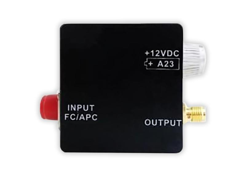 Biased Detector Series PD1500/PD2100
Optical Detectors
Fiberwdm
Wavelength Range: 900nm-1700nm 3dB Cutoff Bandwidth: 5GHz Saturation Optical Power: 5mW
This detector series is a direct replacement for Thorlabs battery-powered products and is described as matching or exceeding equivalent Thorlabs products in all performance aspects. In addition to standard specifications, customization can adjust parameters such as supply voltage and bandwidth to customer requirements. Designed specifically for laser measurement systems, the series has an internal battery and no gain amplification, offering a cost-effective detector for high-power laser laboratories.
-
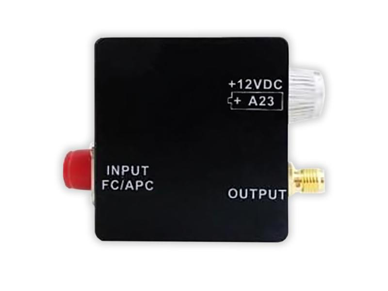 Biased Detector Series PD1500/PD2100
Optical Detectors
Fiberwdm
Wavelength Range: 320nm-1000nm 3dB Cutoff Bandwidth: 1GHz Saturation Optical Power: 5mW
This detector series is a direct replacement for Thorlabs battery-powered products and is described as matching or exceeding equivalent Thorlabs products in all performance aspects. In addition to standard specifications, customization can adjust parameters such as supply voltage and bandwidth to customer requirements. Designed specifically for laser measurement systems, the series has an internal battery and no gain amplification, offering a cost-effective detector for high-power laser laboratories.
-
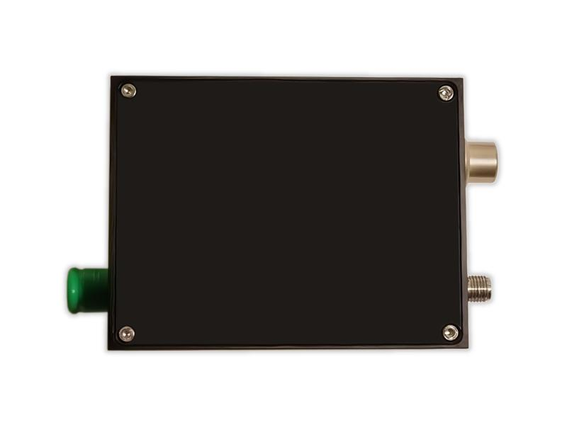 High-Speed Detector HSPD4018
Optical Detectors
Fiberwdm
Wavelength Range: 1000nm - 1700nm 3dB Cutoff Bandwidth: 18GHz Conversion Gain: 35V/W
After nearly two years of R&D,广州瑞东 developed two fully domestic high-speed PD products described as exceeding18GHz and40GHz bandwidth. The18GHz version has rise time<20ps and the40GHz PD<8.5ps. Responsivity is described as matching or exceeding comparable Finisar/Thorlabs imports,with well-controlled tail ringing. Without a TIA,the detectors provide very low noise for high-speed communications and femtosecond-laser testing at high cost effectiveness. The company's independently developed linear supply meets research needs for these detectors.
-
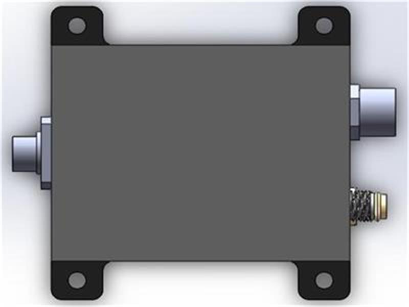 PDA1000-2 Dual-Channel 10KHz Single-Element Detector
Optical Detectors
Fiberwdm
Wavelength Range [Model PDA1000-2 in the Technical Table]: 900-1700nm dB Bandwidth [Model PDA1000-2 in the Technical Table]: 10kHz Conversion Gain [Technical Table Model PDA1000-2; High-Impedance Output Load; Gain Halved from Nominal with 50Ω Load]: 2.5×10⁴V/A
This detector series operates much like single-element detectors from Thorlabs and Newport and has identical power interfaces. It can directly replace equivalent products when Monitor output is unnecessary and bandwidth matches, with performance described as matching or exceeding comparable Thorlabs/Newport detectors. Beyond standard versions, customization adjusts supply voltage, gain, bandwidth and other parameters to customer requirements.
Related Articles
VCSEL, short for Vertical Cavity Surface Emitting Laser, is a widely used semiconductor laser component in modern optoelectronics. Unlike traditional edge-emitting lasers, VCSEL emits laser light vertically from its chip surface. Thanks to its low power consumption, stable beam quality, low cost, and easy integration, it has become the core light source for 3D sensing, wearable devices, and high-speed optical communication.
As fundamental refractive optical components, plano‑convex spherical lenses consist of one convex spherical surface and one flat surface.
FiDAR, the fiber‑optic radar vehicle positioning and tracking system developed by Jianhe Bafang, is a high‑sensitivity distributed fiber‑sensing solution designed for intelligent traffic road monitoring. It outputs real‑time spatial coordinates of every vehicle across the full road section around‑the‑clock, delivering a brand‑new sensing technology for vehicle‑road cooperation, smart highway construction and urban traffic management.
Raybowlaser, a professional manufacturer of high-power laser chips, has officially launched its upgraded new-generation 1470nm high-performance laser chip. Achieving groundbreaking progress in rated output power and wall-plug efficiency (WPE), this innovative laser chip delivers superior and reliable core light source solutions for medical cosmetology, industrial processing, agricultural applications and scientific research equipment.
Loading...
Name
Phone
Organization
Use Case

Database Platform