
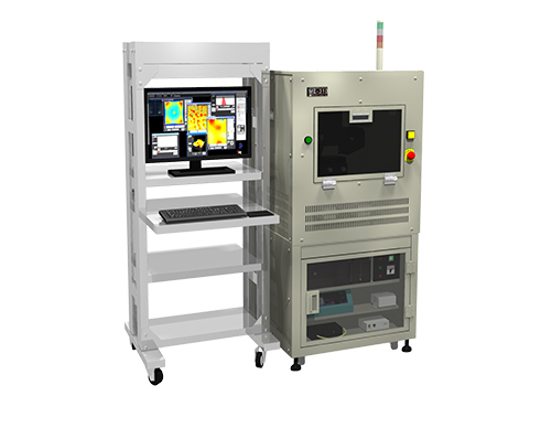
ME-210 High Speed Ellipsometer
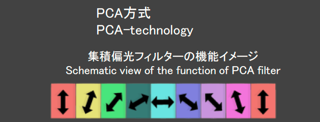
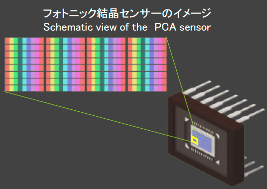
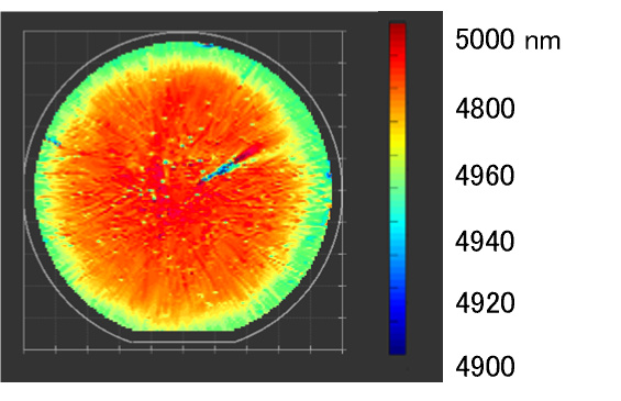
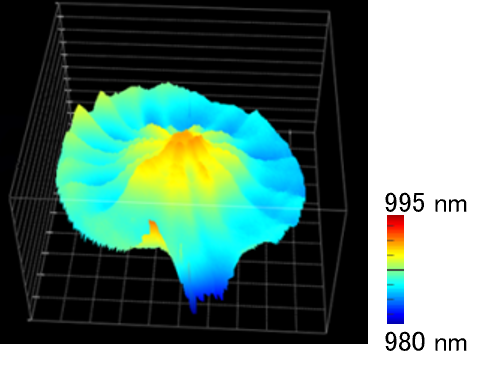
Conventional ellipsometers measure one point at a time, so mapping film thickness uniformity across a surface takes N hours. The minimum measurement resolution is also limited by the laser spot size, preventing film thickness mapping in very small regions. ME-210 overcomes both limitations using a proprietary microscopic polarization array, or photonic crystal.
 Save to Favorites
Overview
Specifications
| Parameter | Value |
|---|---|
| Angle of Incidence | 70 ° |
| Thin Film thickness repetition Accuracy [Standard deviation of 100 repeated measurements at one point on an approximately 100nm SiO2 film on Si] | 0.1 nm |
| Refractive Index Repeatability [Standard deviation of 100 repeated measurements at one point on an approximately 100nm SiO2 film on Si] | 0.001 |
| Measurement speed [Wide Area mode ;100mm Square Shaped Area Measurement] | ≥900 Point / Minutes |
| Measurement speed [High Definition mode ;1mm Square Shaped Area Measurement] | ≥5000 Point / Minutes |
| Light Source | Semiconductor Laser ( Wavelength 636nm) |
| Measurement Point Dimensions [Wide Area mode] | 0.5 mm |
| Measurement Point Dimensions [High Definition mode] | 5.5 μm |
Key Features
Datasheet
Please provide your email to download the datasheet.
Invalid email format. Please try again.
Supplier Information
Related Products
-
PS-3237 wireless polarimeter Optical Metrology Brolight
LED light source: 589 nm Optical-rotation accuracy: ±0.09° Sample-cell length (horizontal direction): 101.3 mm ± 0.8 mm
The PS-3237 wireless polarimeter provides Bluetooth and USB connectivity for analyzing chiral compounds on an iPad®, Chromebook™, Android tablet, or computer. It is ideal for introductory organic-chemistry and biochemistry experiments, where chiral compounds are a major focus. The PASCO wireless polarimeter operates as follows: Plane-polarized light passes through a vertical sample containing a chiral compound, then through an analyzer to a detector. Optical rotation is determined from the angle between the starting position and the position of optimum transmission at the crossed polarizer. Students use rotation data to calculate sample concentration. Specific rotation, the degrees of rotation per gram/milliliter of solution, is an intrinsic property that can distinguish molecules or identify racemic mixtures. In substances with chiral atomic centers, light propagation is anisotropic: Light vibrating in one dimension travels more slowly than light vibrating in another dimension at 90 degrees to it. One component, such as the horizontal component, is slowed, rotating the resultant vibration plane as it passes through the solution. The second polarizer is then rotated until maximum intensity reaches the detector. The angle from its initial to its final orientation is the optical rotation. The polarimeter uses monochromatic light for the following reason: Just as red light is refracted less than violet in a prism, red light is rotated less than orange in an optically active solution, orange less than green, followed by blue and violet. This can be observed with the OS-9477A polarimeter demonstration set: As a crossed polarizer is rotated to transmit the next color through the aligned polarizing arrangement, a Karo syrup solution between two large polarizers changes gradually from red to violet.
-
 Jingli Centering Measurement Instrument Series (Japan) CS-A1100(CS-A1100S)
Optical Metrology
Yuanch
Transmission Centering Measurement Instrument: CS-A1100(CS-A1100S). Uses collimation measurement and an automatic centering navigation system for more accurate and easier centering inspection. Optional software supports statistical analysis and printing. Optional vacuum holding and an automatic rotary stage improve measurement stability for small-aperture lenses. It offers a wide measurement range and good cost effectiveness.
-
Jingli Centering Measurement Instrument Series (Japan) US-A1
Optical Metrology
Yuanch
Reflection Centering Measurement Instrument: US-A1. Developed specifically for small lenses, it uses reflection measurement and a dedicated rotary stage for rapid centering measurement of small-aperture lenses down to φ1mm. It is particularly suitable for endoscope lenses and other small-aperture products.
-
Jingli Centering Measurement Instrument Series (Japan) TR-A1
Optical Metrology
Yuanch
Combined Transmission and Reflection Centering Measurement Instrument: TR-A1. Supports both transmission and reflection measurement modes and a variety of measurement methods. Optional automatic rotation and vacuum holding provide stable measurements.
-
Jingli Centering Measurement Instrument Series (Japan) CS-A3000
Optical Metrology
Yuanch
Transmission Centering Measurement Instrument for Cementing: CS-A3000. Automatically enlarges the display to simplify cementing. Settings can be selected using a touchscreen, with real-time display of centering deviation during operation.
Related Articles
Fomoptic delivers integrated one‑stop optical solutions covering precision optical fabrication and custom vacuum coating services. Supported by complete processing production lines, comprehensive metrology equipment and experienced engineering team, we provide full‑chain customized components, ranging from blank shaping, ultra‑precision polishing to thin‑film coating, for laser systems, infrared imaging, industrial optics and scientific‑research projects.
A solid-state laser is one of the most common and reliable laser types used in modern industry, medical equipment, and scientific research. Unlike gas or fiber lasers, it uses solid materials as its gain medium to generate stable, high-brightness laser beams. Thanks to its high precision, long lifespan, and compact structure, solid-state lasers have become a mainstream solution for high-precision laser processing and optical systems.
In photonics and laser technology, devices that manipulate optical signals via the electro-optic effect form the backbone of precision optical systems. Electro-optic phase modulators and electro-optic deflectors are two prominent examples of this device category. As a critical hardware solution for high-speed, high-accuracy laser beam direction control, electro-optic deflectors are widely deployed across industrial and research settings. Below is a detailed overview of their core structure, key performance drivers, and primary use cases.
In UV laser testing, UV spectroscopy and lithography optical experiments, excessive light intensity will lead to detector saturation, optical component damage and overexposed imaging.
Loading...
Name
Phone
Organization
Use Case

Database Platform