
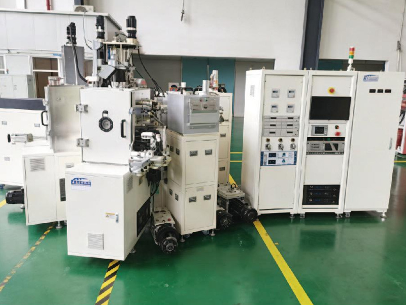
Cluster multifunctional thin-film deposition system (Cluster)
The equipment coats substrates up to 300mmX300mm. Its compact cluster layout places a transfer chamber centrally and functional coating chambers around it for easy substrate transfer. Peripheral chambers can be configured for evaporation, magnetron sputtering, plasma cleaning, or other functions to customer requirements.
 Save to Favorites
Overview
Specifications
| Parameter | Value |
|---|---|
| Transfer chamber and transfer robot arm - Ultimate vacuum | 8E-5Pa |
| Transfer chamber and transfer robot arm - Robot sample-transfer positioning accuracy | ±0.2mm |
| Sample loading/unloading chamber (loadlock) - Ultimate vacuum | 8E-5Pa |
| Sample loading/unloading chamber (loadlock) - Cassette [Standards] | 10layers |
| Evaporation-deposition chamber - Ultimate vacuum | 4E-5Pa |
| Evaporation-deposition chamber - Substrate-stage mechanical alignment accuracy | ±0.2mm |
| Evaporation-deposition chamber - CCD alignment accuracy | ±5um |
| High-temperature evaporation-deposition chamber - Ultimate vacuum | 4E-5Pa |
| High-temperature evaporation-deposition chamber - Substrate-stage mechanical alignment accuracy | ±0.2mm |
| Rotating chamber | 90 degrees, 180 degrees and 270 degrees |
| Inverting chamber | 180degrees |
| Heating/bakeout chamber | Heating and bakeout degassing of substrates or MASK |
| Test data (film-thickness uniformity) - Target rate | 2A/S |
| Test data (film-thickness uniformity) - Experimental data 1 - Sequence number - 1 [Target Rate: 2A/S] | 760.1 |
| Test data (film-thickness uniformity) - Experimental data 1 - Sequence number - 2 [Target Rate: 2A/S] | 777.95 |
| Test data (film-thickness uniformity) - Experimental data 1 - Sequence number - 3 [Target Rate: 2A/S] | 774.6 |
| Test data (film-thickness uniformity) - Experimental data 1 - Sequence number - 4 [Target Rate: 2A/S] | 788.4 |
| Test data (film-thickness uniformity) - Experimental data 1 - Sequence number - 5 [Target Rate: 2A/S] | 800.8 |
| Test data (film-thickness uniformity) - Experimental data 1 - Sequence number - 6 [Target Rate: 2A/S] | 799.4 |
| Test data (film-thickness uniformity) - Experimental data 1 - Sequence number - 7 [Target Rate: 2A/S] | 797.05 |
| Test data (film-thickness uniformity) - Experimental data 1 - Sequence number - 8 [Target Rate: 2A/S] | 788.7 |
| Test data (film-thickness uniformity) - Experimental data 1 - Sequence number - 9 [Target Rate: 2A/S] | 776.75 |
| Test data (film-thickness uniformity) - Experimental data 1 - Sequence number - 10 [Target Rate: 2A/S] | 762.95 |
| Test data (film-thickness uniformity) - Experimental data 1 - Sequence number - 11 [Target Rate: 2A/S] | 747.3 |
| Test data (film-thickness uniformity) - Experimental data 1 - Sequence number - 12 [Target Rate: 2A/S] | 775.95 |
| Test data (film-thickness uniformity) - Experimental data 1 - Sequence number - 13 [Target Rate: 2A/S] | 777 |
| Test data (film-thickness uniformity) - Experimental data 1 [Target Rate: 2A/S] | min:747.3; max:800.8 |
| Test data (film-thickness uniformity) - Experimental data 1 - Uniformity [Target Rate: 2A/S] | 0.03456 |
| Test data (film-thickness uniformity) - Experimental data 2 - Sequence number - 1 [Target Rate: 2A/S] | 1090.95 |
| Test data (film-thickness uniformity) - Experimental data 2 - Sequence number - 2 [Target Rate: 2A/S] | 1106.5 |
| Test data (film-thickness uniformity) - Experimental data 2 - Sequence number - 3 [Target Rate: 2A/S] | 1115.25 |
| Test data (film-thickness uniformity) - Experimental data 2 - Sequence number - 4 [Target Rate: 2A/S] | 1131.6 |
| Test data (film-thickness uniformity) - Experimental data 2 - Sequence number - 5 [Target Rate: 2A/S] | 1142.9 |
| Test data (film-thickness uniformity) - Experimental data 2 - Sequence number - 6 [Target Rate: 2A/S] | 1140.45 |
| Test data (film-thickness uniformity) - Experimental data 2 - Sequence number - 7 [Target Rate: 2A/S] | 1130.4 |
| Test data (film-thickness uniformity) - Experimental data 2 - Sequence number - 8 [Target Rate: 2A/S] | 1115.05 |
| Test data (film-thickness uniformity) - Experimental data 2 - Sequence number - 9 [Target Rate: 2A/S] | 1105.85 |
| Test data (film-thickness uniformity) - Experimental data 2 - Sequence number - 10 [Target Rate: 2A/S] | 1106.75 |
| Test data (film-thickness uniformity) - Experimental data 2 - Sequence number - 11 [Target Rate: 2A/S] | 1088.35 |
| Test data (film-thickness uniformity) - Experimental data 2 - Sequence number - 12 [Target Rate: 2A/S] | 1087.55 |
| Test data (film-thickness uniformity) - Experimental data 2 - Sequence number - 13 [Target Rate: 2A/S] | 1093 |
| Test data (film-thickness uniformity) - Experimental data 2 [Target Rate: 2A/S] | min:1087.55; max:1142.9 |
| Test data (film-thickness uniformity) - Experimental data 2 - Uniformity [Target Rate: 2A/S] | 0.02482 |
| Test data (film-thickness uniformity) - Experimental data 3 - Sequence number - 1 [Target Rate: 2A/S] | 673.8 |
| Test data (film-thickness uniformity) - Experimental data 3 - Sequence number - 2 [Target Rate: 2A/S] | 679.4 |
| Test data (film-thickness uniformity) - Experimental data 3 - Sequence number - 3 [Target Rate: 2A/S] | 688.15 |
| Test data (film-thickness uniformity) - Experimental data 3 - Sequence number - 4 [Target Rate: 2A/S] | 692 |
| Test data (film-thickness uniformity) - Experimental data 3 - Sequence number - 5 [Target Rate: 2A/S] | 697 |
| Test data (film-thickness uniformity) - Experimental data 3 - Sequence number - 6 [Target Rate: 2A/S] | 698.8 |
| Test data (film-thickness uniformity) - Experimental data 3 - Sequence number - 7 [Target Rate: 2A/S] | 694.55 |
| Test data (film-thickness uniformity) - Experimental data 3 - Sequence number - 8 [Target Rate: 2A/S] | 690.3 |
| Test data (film-thickness uniformity) - Experimental data 3 - Sequence number - 9 [Target Rate: 2A/S] | 686.7 |
| Test data (film-thickness uniformity) - Experimental data 3 - Sequence number - 10 [Target Rate: 2A/S] | 678.05 |
| Test data (film-thickness uniformity) - Experimental data 3 - Sequence number - 11 [Target Rate: 2A/S] | 669.6 |
| Test data (film-thickness uniformity) - Experimental data 3 - Sequence number - 12 [Target Rate: 2A/S] | 704.85 |
| Test data (film-thickness uniformity) - Experimental data 3 - Sequence number - 13 [Target Rate: 2A/S] | 689.7 |
| Test data (film-thickness uniformity) - Experimental data 3 [Target Rate: 2A/S] | min:669.6; max:704.85 |
| Test data (film-thickness uniformity) - Experimental data 3 - Uniformity [Target Rate: 2A/S] | 0.02565 |
Applications
Datasheet
Please provide your email to download the datasheet.
Invalid email format. Please try again.
Supplier Information
Related Products
-
 Post-Evaporation Inspection System
Semiconductor Manufacturing Equipment
Lic-vision
-
 Lithography System
Semiconductor Manufacturing Equipment
Trusee
-
 Resist Stripping System
Semiconductor Manufacturing Equipment
Trusee
-
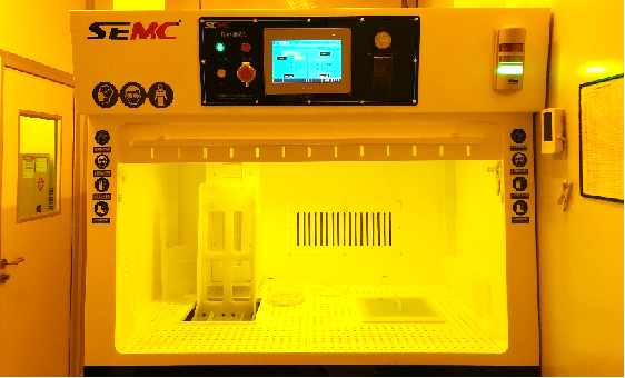 Developing System
Semiconductor Manufacturing Equipment
Trusee
-
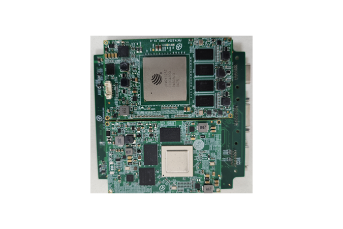 Image Recognition and Tracking Board
Semiconductor Manufacturing Equipment
Tera-aurora
Main Processor [FPGA]: Fudan Micro 7K325t Main Processor [ARM]: HiSilicon 3403 Storage [FPGA]: 32G EMMC, 64G SD Card
Image Recognition and Tracking Board
Related Articles
VCSEL, short for Vertical Cavity Surface Emitting Laser, is a widely used semiconductor laser component in modern optoelectronics. Unlike traditional edge-emitting lasers, VCSEL emits laser light vertically from its chip surface. Thanks to its low power consumption, stable beam quality, low cost, and easy integration, it has become the core light source for 3D sensing, wearable devices, and high-speed optical communication.
As fundamental refractive optical components, plano‑convex spherical lenses consist of one convex spherical surface and one flat surface.
FiDAR, the fiber‑optic radar vehicle positioning and tracking system developed by Jianhe Bafang, is a high‑sensitivity distributed fiber‑sensing solution designed for intelligent traffic road monitoring. It outputs real‑time spatial coordinates of every vehicle across the full road section around‑the‑clock, delivering a brand‑new sensing technology for vehicle‑road cooperation, smart highway construction and urban traffic management.
Raybowlaser, a professional manufacturer of high-power laser chips, has officially launched its upgraded new-generation 1470nm high-performance laser chip. Achieving groundbreaking progress in rated output power and wall-plug efficiency (WPE), this innovative laser chip delivers superior and reliable core light source solutions for medical cosmetology, industrial processing, agricultural applications and scientific research equipment.
Loading...
Name
Phone
Organization
Use Case

Database Platform