
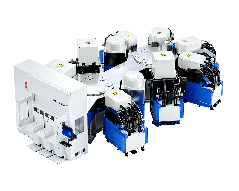
Cluster coating platform
ICP-assisted magnetron sputtering produces low-absorption, low-stress optical coatings for various bandpass and cutoff applications, such as face recognition (Face lD) and high-transmission mid- and far-infrared coatings. Magnetron sputtering deposits metals such as Cu, Al, Cr, Au, Ag and SUS. Process development improves deep-hole coating, providing excellent step coverage for MEMS chip packaging. Modular equipment can combine Plasma-clean, magnetron sputtering (SPT), plasma-enhanced chemical reaction (PECVD), atomic layer deposition (ALD) and reactive-ion etching (RIE) units into a cluster processing center covering substrate cleaning, thin-film deposition including ultrathin films, and patterned etching for semiconductor micro- and nanostructures. It meets stringent deposition-uniformity specifications, minimizes high-stress film defects, improves throughput and reduces costs.
 Save to Favorites
Overview
Specifications
| Parameter | Value |
|---|---|
| Wafer loading capacity [Wafer size 4″] | 16 |
| Wafer loading capacity [Wafer size 6″] | 12 |
| Wafer loading capacity [Wafer size 8″] | 9 |
| Wafer loading capacity [Wafer size 12″] | 5 |
Applications
Key Features
Datasheet
Please provide your email to download the datasheet.
Invalid email format. Please try again.
Supplier Information
Related Products
-
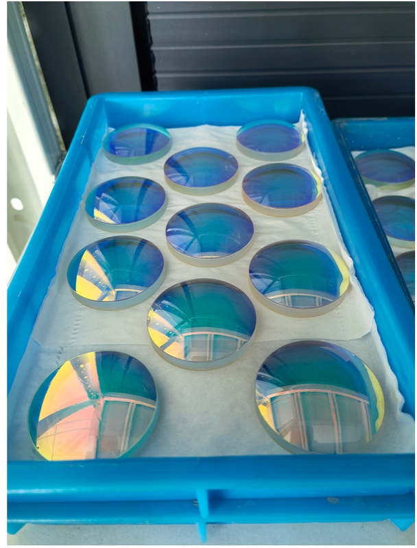 Coated Component
Material-based Production Equipment
Fuzhouzhiyi
-
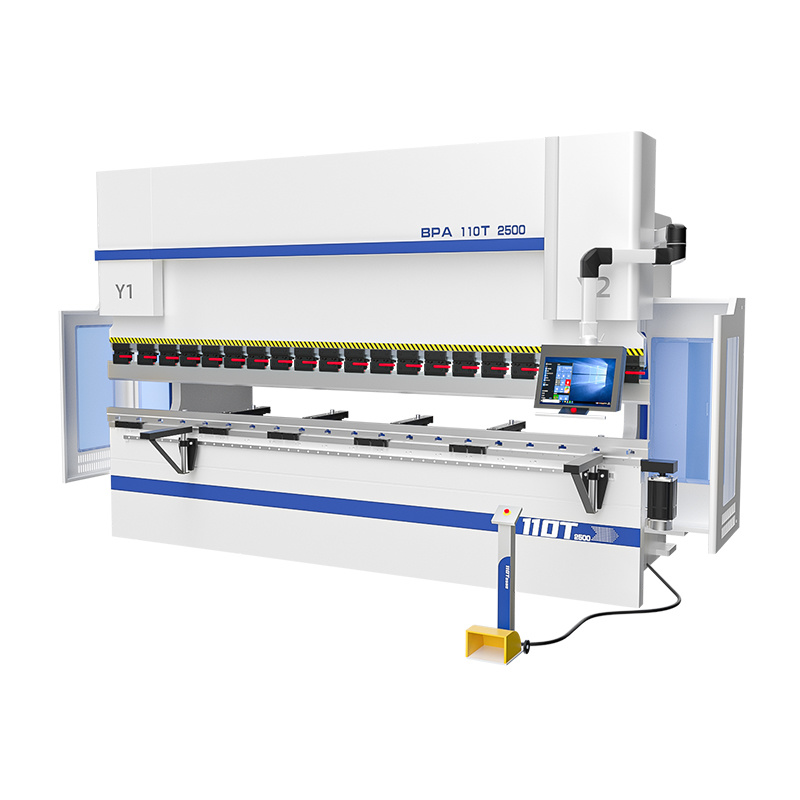 Electro-Hydraulic Synchronous CNC Press Brake Machine 80T2500
Material-based Production Equipment
Auroralaser
Bending Capacity: 800 kN Bending Length: 2500 mm Distance Between Columns: 2000 mm
The Electro-Hydraulic Synchronous CNC Press Brake employs a high-precision electro-hydraulic control system and robust frame to ensure efficient, stable processing of complex bends, significantly enhancing production accuracy and profitability.
-
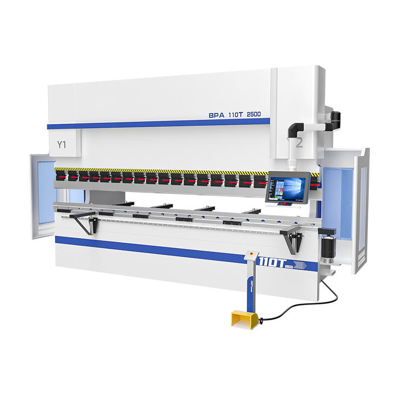 Electro-Hydraulic Synchronous CNC Press Brake Machine 110T2500
Material-based Production Equipment
Auroralaser
Bending Capacity: 1100 kN Bending Length: 2500 mm Distance Between Columns: 2000 mm
The Electro-Hydraulic Synchronous CNC Press Brake employs a high-precision electro-hydraulic control system and robust frame to ensure efficient, stable processing of complex bends, significantly enhancing production accuracy and profitability.
-
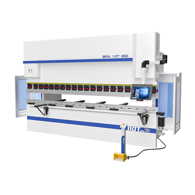 Electro-Hydraulic Synchronous CNC Press Brake Machine 110T4100
Material-based Production Equipment
Auroralaser
Bending Capacity: 1100 kN Bending Length: 4100 mm Distance Between Columns: 3500 mm
The Electro-Hydraulic Synchronous CNC Press Brake employs a high-precision electro-hydraulic control system and robust frame to ensure efficient, stable processing of complex bends, significantly enhancing production accuracy and profitability.
-
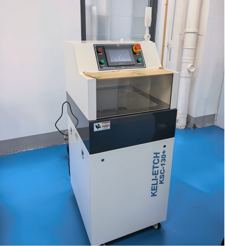 Wafer Bonding
Material-based Production Equipment
Jmwafer
晶沐光电 combines wafer grinding/polishing/thinning and laser processing to provide homogeneous/heterogeneous, permanent/temporary wafer bonding. High vacuum sealing, heat/pressure and surface activation create reliable interfaces for3D integration, advanced packaging, MEMS, power, RF and optoelectronic devices, including custom small batches for institutes. Referenced processes/equipment include single-wafer cleaning, class100 cleanroom bonding and KSB-H1000. Permanent bonding irreversibly joins wafers/chips into strong, hermetic, reliable structures. Direct bonding uses ultracleaning, plasma activation and CMP, room-temperature van der Waals prebonding and annealed Si-O-Si covalent bonds: no interlayer, high strength/hermeticity/insulation, void-free/low-stress interfaces for Si/Si, Si/SiO2 and Si/SOI. Anodic bonding uses heat/high electric field for silicon–glass chemical bonds, near-bulk strength, low leak rate and stable sealed cavities, such as Si/borosilicate. Eutectic bonding melts/diffuses Au-Sn, Cu-Sn, In or Au-Si interlayers, yielding low-temperature, conductive, thermally conductive, reliable bonds with broad process windows for Cu/Au/Sn-coated wafers. Thermocompression uses heat/precise pressure for solder-free metal-atom diffusion, high interconnect density/low interface resistance, and direct bonding of Si, metal-coated, compound-semiconductor, sapphire, glass, SiC or ceramic wafers. Hybrid bonding simultaneously joins copper/dielectric for integrated mechanical/electrical submicron-pitch connections, high bandwidth, low latency/loss and HBM/AI stacking in3D NAND, HBM, AI processors, high-end Chiplets and VLSI wafers. Examples are sapphire/Si, SiO2/sapphire and GaAs/Si. Temporary bonding glues a wafer/chip to a carrier for backside processing then gentle release. Thermal-slide bonding softens thermoplastics, PPC or polyimides with heat, hardens on cooling and reheats/slides for release; it resists heat/chemicals for Si thinning, TSV and advanced packaging, but needs heating and may leave adhesive. UV release cures for strength then shortwave UV degrades/debonds UV-release adhesive/double-sided tape: gentle room-temperature release for heat-sensitive MEMS, CIS, compound and ultrathin wafers, but needs a transparent carrier and has moderate heat resistance. Laser release uses transparent carriers and an absorbing layer to decompose/release adhesive without contact; laser-responsive coating plus bonding adhesive gives stress-free, residue-free, precise release for large ultrathin3D IC/HBM/Chiplet/advanced-packaging wafers, at high equipment/material cost. Low-melting In, SnBi or AuSn alloys bond molten and remelt for release; high heat tolerance/conductivity and acid/alkali resistance suit SiC/GaN power devices/high-temperature processes, but metal residue is difficult to clean and processing is complex. Bondable materials include Si, SiC, GaN, sapphire, GaAs, InP, quartz/borosilicate glass, alumina/aluminum-nitride ceramics, diamond, bonded composites, SOI, lithium tantalate/niobate and coated wafers.
Related Articles
In photonics and laser technology, devices that manipulate optical signals via the electro-optic effect form the backbone of precision optical systems. Electro-optic phase modulators and electro-optic deflectors are two prominent examples of this device category. As a critical hardware solution for high-speed, high-accuracy laser beam direction control, electro-optic deflectors are widely deployed across industrial and research settings. Below is a detailed overview of their core structure, key performance drivers, and primary use cases.
GYOPTICS 30 W collimated isolator is a highly‑reliable passive optical component optimized for 1064 nm high‑power laser systems. Characterized by low insertion loss and superior backward‑light suppression capability, it effectively blocks reflected light traveling back toward the laser resonator, eliminating back‑reflection‑induced instability and protecting fiber or solid‑state laser sources during long‑term operation.
For 1D optical detection scenarios such as spectrum acquisition, dimensional measurement and optical scanning, area array CMOS/CCD suffer redundant pixels, high cost and slow row readout speed.
Laser pump sources are the core energy input component of solid-state lasers and laser amplifiers, and their performance directly determines the output power, beam quality and service life of the entire laser system. In scenarios such as industrial processing, scientific research experiments and high-end equipment, improper pump source selection will not only result in substandard system performance, but also bring a series of problems such as rapid device degradation and high operation and maintenance costs. This article sorts out the core selection logic and key pitfalls of pump source procurement, and provides selection references based on mature, mass-produced high-reliability products to help purchasers efficiently screen suitable products.
Loading...
Name
Phone
Organization
Use Case

Database Platform