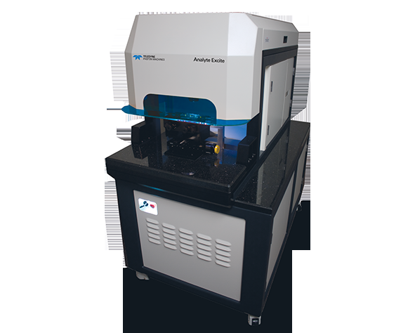
Analyte Excit System is Based on Analyte G2 System , Update on Upgrade Development Ultrashort Pulse Laser Ablation System , It can decimate all samples. , And it's got a super high value for money. 。Excit The system has a fine control unit , High-energy. “ Flattop ” Laser And the speed response. “ Side to side. ” It's... (“shot-to-shot”)“ Dynamic Erosion function ”, High resolution space analysis capability 。 Breakthrough technology " Dynamic Erosion function " (“Fire-on-the-fly”) High Resolution X-Y Mobile platform technology , And the motion platform can be activated in real time. Laser Fire , Perfectly applied to the depths of the line scan and the analysis of the distribution of the elements. 。Excit System uses high resolution GigE Real-colour micro-image observation technology. , Optical resolution of observation unit <2μm, Provides a trans-radiation 、 Reflection and Ring Adjustable Lighting and cross-distortion systems for brightness , It's real time enough to show real time scaling. Dynamic The wide field of view. , Quick sample positioning navigation 。 Gather! Ultrashort Pulse (<5ns) It's... 193nm Wavelength Gas Excimer Wavelength It's... Laser Ablation System , is None Application range of superior and efficient erosion 。 And the width Pulse (20+ns)193nm Laser System comparison ,Excit The system can produce higher. “ Peak Power ”, It's easier to skin samples. , Generate more finer aerosols. , And you get smaller ripping and distillation effects. , Promote ICP The Analytical Signal Is More Stable 。Excit The system can decipher all samples. , Erosion of transparent samples to more transparent samples , Such as High Purity Quartz 、 Flex carbonate samples, etc. , One-time decorate depth. 10 Donami. 。Excit System specification 30 A ripping spot. , Spot range 1μm -~150μm。
| Parameter | Value |
|---|
| Laser Wavelength | 193nm |
| Ultrashort Pulse | <4ns/pulse |
| Energy density | Maximum 15J/cm² |
| Mobile Platform | 100mmx100mm |
| Rip the light range. | ∽1μm-150μm |
| Erosion flares | Plot 30 individual , of which 20 Circle 、6 Squares and 4 A narrow slit. ; Light spots Customizable |
Analysis of environmental samples Analysis of the analysis of the qualitative analysis of the isotopes of agricultural samples by physical samples and analysis of the qualitative analysis of the biological samples by the general volume sample and analysis of the geological samples by the mapping of the fault analysis elements of the samples by the analysis of the transparent and semi-transparent sample analysis by the deep decorative analysis of the mineral samples Inert gas isotopes / Stabilizing isotope analysis sample types : The Quest / Man-suk! / Skullstone. 、 Metal Totals 、 Transparent and translucent samples 、 Bones. 、 Teeth and fur, etc. 、 Ceramic 、 Plastic 、 Ultrathin Painting / Placing 、 Minerals of all types 、 Animal and plant tissues, etc.
Best value for money. 193nm Laser Ablation System · The super-shock-proof platform. · Ultrashort Pulse 193nm Wavelength · Ultrashort Pulse <4ns/pulse · Sufficient energy density to decimate samples. , Maximum 15J/cm² ·ArF Seal the bottle. Vapor Cell · Best “ Zero. ” & Filter , Best Dynamic & Harmonize , Best “ Flattop ” Laser · Optical Attenuator is “Open Gate” Functions , Allows Laser “100%” Pass. ·“ Sync Dynamic Erosion function ” Elemental erosion and distribution maps that reach perfect control depth · Plot 100mmx100mm Mobile Platform · Independent video and Laser Optical control unit , Provides a Good Field of View and Better Ablation Crater Quality · Rip the light range. ∽ 1μm -150μm · Plot 30 A fragrance. , of which 20 Circle 、6 Squares and 4 A narrow slit. ; Light spots Customizable · The best decorating ponds of the day. HelExⅡ Double-sized double-air-flow sample pool · Support upgrading to Femtosecond Laser Ablation System
Please provide your email to download the datasheet.
Suzhou H&L Instruments Co., Ltd. is located in Suzhou, the geographic center of the fertile Yangtze River Delta. It is an optical precision measurement instrument company dedicated to the integration of optics, mechanics, electronics and software and integrated system design. Founded in March 2009, the company's goal is to industrialize internationally leading optical testing technology and lead the development trend of the optical testing industry.
The H&L Instruments team has more than 30 years of R&D and engineering experience in the field of optical testing. Projects and products completed at home and abroad include: the development and application of the world's first 24-inch aperture phase-shifting interferometer, the development and application of ultra-high-precision interferometers for key components in the LIGO gravitational wave detection project, chip testing technology and engineering, the development and application of semiconductor-specific equipment for measuring wafer flatness and thickness variation, and more than 20 domestic and international scientific research and engineering projects including national major instrument and equipment special projects and industrialization, with total R&D funding of hundreds of millions of yuan, forming an R&D system centered on the integration of optics, mechanics, electronics and software.
Adopting a modular design concept and combining decades of R&D experience, H&L Instruments has developed digital high-precision laser interferometer modules with independent intellectual property rights. On this basis, three types of interferometers have been formed, including: stress-free plane testing interferometers, on-site high-efficiency spherical testing interferometers, and general combined horizontal interferometers. They can cover multiple apertures and feature modularity, high precision, high efficiency, 100% non-destructiveness, and strong anti-interference performance. Since its establishment, the company has continuously advanced its technology and updated its products, with more than ten product iterations so far, and instrument performance has reached the international advanced level.
Digital high-precision laser interferometers are mainly used to detect topography errors of high-precision machined surfaces, solving the applicability and practicality problems of existing similar instruments, and have been successfully applied in fields such as metrology testing, industrial processing sites, scientific research, and teaching instruments in colleges and universities. At the same time, the company has expanded into market segments such as wafer testing in the semiconductor industry, flat panel testing in large flat panel displays, data storage, smooth component surface testing in MEMS/NEMS industry, nano-thin material testing, and LED chip fabrication.
During its development, H&L Instruments has continuously carried out exchanges and cooperation with many domestic and foreign research institutions such as the College of Optical Sciences of the University of Arizona in the United States, the Institute of Optics of the University of Stuttgart in Germany, and the School of Optical-Electrical and Computer Engineering of the University of Shanghai for Science and Technology. It has achieved long-term and effective development in project development, scientific research improvement, and talent training, rapidly improving its design and production, maintenance and debugging, and engineering transformation capabilities, and continuously expanding its scale.
Today, the employees of H&L Instruments uphold the belief of "enterprising, realistic, rigorous, united", continuously explore and innovate, take technology as the core, regard quality as life, and treat customers as God, and are dedicated to providing customers with the most cost-effective digital high-precision laser interferometers and their system application solutions.

 Save to Favorites


