
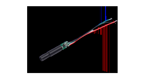
Positioning Marking
Semiconductor Positioning Marking is is. Semiconductor A technique used in the production process , By the Wafer Mark unique identifiers , To help equipment and systems identify and locate accurately Wafer , This will increase productivity 。 Semiconductor Positioning Marking The role of the organization is mainly as follows: : 1. Increase Wafer Accuracy and stability : Semiconductor Positioning Marking Ensures the Equipment When Processing Wafer It can be located and identified accurately. Wafer Position and Direction , So as to avoid production problems caused by location deviations or misdirection , Promise. Wafer Accuracy and stability 。 2. Increased efficiency and reduced costs of production : Pass. Semiconductor Positioning Marking , Production equipment can be located and identified more quickly Wafer , Increased efficiency and speed of production 。 Besides , By reducing the generation of waste products caused by mispositioning , It reduces production costs. 。 3. Increase Wafer Identification capability : Semiconductor Positioning Marking is. Wafer Mark unique identifiers , Helping devices to distinguish between different Wafer , To enable the production process to be based on Wafer Type and needs of the project are addressed accordingly , Increase Wafer Identification capability 。 4. Optimizing production processes and improving production quality : Pass. Semiconductor Positioning Marking , It's achievable. Wafer Automation of positioning and management in the production process , So that production process can be optimized , Improving the quality of production , Reducing production errors and problems 。 Overall , Semiconductor Positioning Marking It can improve production efficiency , Improving the quality of production , Reducing production costs , And it helps. Semiconductor Production enterprises to improve competitiveness and market share 。 In future development , With Semiconductor The continuous evolution of industry and the upgrading of technology , Semiconductor Positioning Marking It's going to be more important. , Yeah. Semiconductor And the impact of production will be increasing. 。
 Save to Favorites
Overview
Datasheet
Please provide your email to download the datasheet.
Invalid email format. Please try again.
Supplier Information
Related Products
-
Fiber for Helium-Neon Laser Therapy System SMA-UVHN-01 Laser Modules & Systems Fiberock
Optical fiber material: UV silica fiber Connector Type: SMA905/FC/custom Fiber core count: Single-core
Neon laser therapy instruments (Helium-Neon, He-Ne, laser devices) were among the early lasers used therapeutically and are known for their Low-Level Laser Therapy (LLLT) effects on tissue. He-Ne lasers mainly emit red light at 632.8 nanometers, beneficial for certain tissue treatments such as wound healing, inflammation reduction, pain relief, and cellular repair. In medical applications, specially designed high-quality medical fibers often deliver He-Ne light to target body areas without significant power loss. Fibers allow flexible application throughout the body regardless of the laser's position. 1. Compatibility: the fiber input must match the laser-emitting equipment interface. 2. Transmission loss: losses should be minimized to deliver sufficient energy to the treatment area. 3. Flexibility and durability: fibers should accommodate different clinical situations and conditions. 4. Safety: accurate beam delivery and prevention of leakage protect patients and healthcare personnel. 5. Beam quality: fibers must maintain beam quality during transmission to avoid reduced effectiveness from defocusing or mode mismatch. He-Ne lasers have gradually been replaced by other lasers, such as high-power semiconductor lasers, which are generally more compact, efficient, and inexpensive to maintain. Nevertheless, He-Ne lasers retain a distinctive role in low-level laser therapy for certain treatments.
-
Fiber for Helium-Neon Laser Therapy System SMA-UVHN-02 Laser Modules & Systems Fiberock
Optical fiber material: UV silica fiber Connector Type: SMA905/FC/custom Fiber core count: Multicore
Neon laser therapy instruments (Helium-Neon, He-Ne, laser devices) were among the early lasers used therapeutically and are known for their Low-Level Laser Therapy (LLLT) effects on tissue. He-Ne lasers mainly emit red light at 632.8 nanometers, beneficial for certain tissue treatments such as wound healing, inflammation reduction, pain relief, and cellular repair. In medical applications, specially designed high-quality medical fibers often deliver He-Ne light to target body areas without significant power loss. Fibers allow flexible application throughout the body regardless of the laser's position. 1. Compatibility: the fiber input must match the laser-emitting equipment interface. 2. Transmission loss: losses should be minimized to deliver sufficient energy to the treatment area. 3. Flexibility and durability: fibers should accommodate different clinical situations and conditions. 4. Safety: accurate beam delivery and prevention of leakage protect patients and healthcare personnel. 5. Beam quality: fibers must maintain beam quality during transmission to avoid reduced effectiveness from defocusing or mode mismatch. He-Ne lasers have gradually been replaced by other lasers, such as high-power semiconductor lasers, which are generally more compact, efficient, and inexpensive to maintain. Nevertheless, He-Ne lasers retain a distinctive role in low-level laser therapy for certain treatments.
-
Fiber for Helium-Neon Laser Therapy System SMA-DUVHN-01 Laser Modules & Systems Fiberock
Optical fiber material: UV-Resistant Silica Fiber Connector Type: SMA905/FC/custom Fiber core count: Single-core
Neon laser therapy instruments (Helium-Neon, He-Ne, laser devices) were among the early lasers used therapeutically and are known for their Low-Level Laser Therapy (LLLT) effects on tissue. He-Ne lasers mainly emit red light at 632.8 nanometers, beneficial for certain tissue treatments such as wound healing, inflammation reduction, pain relief, and cellular repair. In medical applications, specially designed high-quality medical fibers often deliver He-Ne light to target body areas without significant power loss. Fibers allow flexible application throughout the body regardless of the laser's position. 1. Compatibility: the fiber input must match the laser-emitting equipment interface. 2. Transmission loss: losses should be minimized to deliver sufficient energy to the treatment area. 3. Flexibility and durability: fibers should accommodate different clinical situations and conditions. 4. Safety: accurate beam delivery and prevention of leakage protect patients and healthcare personnel. 5. Beam quality: fibers must maintain beam quality during transmission to avoid reduced effectiveness from defocusing or mode mismatch. He-Ne lasers have gradually been replaced by other lasers, such as high-power semiconductor lasers, which are generally more compact, efficient, and inexpensive to maintain. Nevertheless, He-Ne lasers retain a distinctive role in low-level laser therapy for certain treatments.
-
Fiber for Helium-Neon Laser Therapy System SMA-DUVHN02 Laser Modules & Systems Fiberock
Optical fiber material: UV-Resistant Silica Fiber Connector Type: SMA905/FC/custom Fiber core count: Multicore
Neon laser therapy instruments (Helium-Neon, He-Ne, laser devices) were among the early lasers used therapeutically and are known for their Low-Level Laser Therapy (LLLT) effects on tissue. He-Ne lasers mainly emit red light at 632.8 nanometers, beneficial for certain tissue treatments such as wound healing, inflammation reduction, pain relief, and cellular repair. In medical applications, specially designed high-quality medical fibers often deliver He-Ne light to target body areas without significant power loss. Fibers allow flexible application throughout the body regardless of the laser's position. 1. Compatibility: the fiber input must match the laser-emitting equipment interface. 2. Transmission loss: losses should be minimized to deliver sufficient energy to the treatment area. 3. Flexibility and durability: fibers should accommodate different clinical situations and conditions. 4. Safety: accurate beam delivery and prevention of leakage protect patients and healthcare personnel. 5. Beam quality: fibers must maintain beam quality during transmission to avoid reduced effectiveness from defocusing or mode mismatch. He-Ne lasers have gradually been replaced by other lasers, such as high-power semiconductor lasers, which are generally more compact, efficient, and inexpensive to maintain. Nevertheless, He-Ne lasers retain a distinctive role in low-level laser therapy for certain treatments.
-
Fiber for Helium-Neon Laser Therapy System SMA-IRHN-01 Laser Modules & Systems Fiberock
Optical fiber material: Infrared silica fiber Connector Type: SMA905/FC/custom Fiber core count: Single-core
Neon laser therapy instruments (Helium-Neon, He-Ne, laser devices) were among the early lasers used therapeutically and are known for their Low-Level Laser Therapy (LLLT) effects on tissue. He-Ne lasers mainly emit red light at 632.8 nanometers, beneficial for certain tissue treatments such as wound healing, inflammation reduction, pain relief, and cellular repair. In medical applications, specially designed high-quality medical fibers often deliver He-Ne light to target body areas without significant power loss. Fibers allow flexible application throughout the body regardless of the laser's position. 1. Compatibility: the fiber input must match the laser-emitting equipment interface. 2. Transmission loss: losses should be minimized to deliver sufficient energy to the treatment area. 3. Flexibility and durability: fibers should accommodate different clinical situations and conditions. 4. Safety: accurate beam delivery and prevention of leakage protect patients and healthcare personnel. 5. Beam quality: fibers must maintain beam quality during transmission to avoid reduced effectiveness from defocusing or mode mismatch. He-Ne lasers have gradually been replaced by other lasers, such as high-power semiconductor lasers, which are generally more compact, efficient, and inexpensive to maintain. Nevertheless, He-Ne lasers retain a distinctive role in low-level laser therapy for certain treatments.
Related Articles
The LZFL405‑80mW‑3 series from Shenzhen Leirte Optoelectronics Co., Ltd. is a coaxial‑packaged violet‑blue single‑mode fiber‑coupled laser diode. It delivers 80 mW continuous‑wave output at 405 nm. Light is coupled into 3 μm core‑diameter single‑mode fiber for clean beam quality and easy integration into diverse optical systems. It serves as a compact violet‑blue light source for medical instruments and industrial printing applications.
Macro channel water-cooled stacked laser diodes integrate dozens of laser bars into one vertical stacked module with large-diameter macro flow cooling channels.
CytoViva delivers comprehensive hyperspectral imaging solutions covering visible to near-infrared spectrum, compatible with brightfield, fluorescence and proprietary enhanced darkfield microscopy modes.
Electro-optic deflectors (EODs) are optical devices used to steer or deflect light beams by applying an electric field to a specialized optical crystal. Unlike mechanical beam steering systems that rely on moving mirrors, electro-optic deflectors enable high-speed, non-mechanical beam control with exceptional precision and responsiveness. They are widely used in laser scanning, optical communications, microscopy, laser printing, spectroscopy, and scientific research, where rapid and accurate laser beam positioning is essential.
Loading...
Name
Phone
Organization
Use Case

Database Platform