
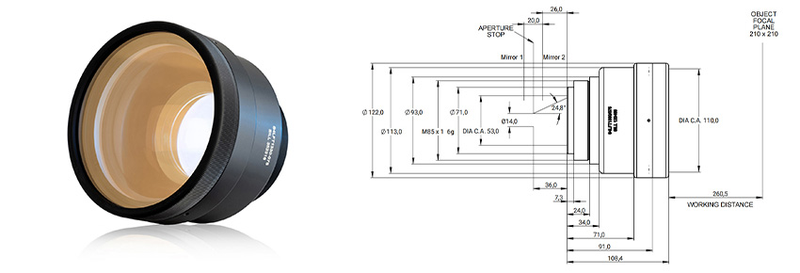
f-theta Scanning Lens for Photovoltaic Applications S4LFT1330-075
The energy transition presents global challenges, making renewable energy sources such as photovoltaics essential. A key to improving photovoltaic efficiency is to improve solar-cell manufacturing. Laser material processing is used to weld individual cells into modules, dope selective emitters, and remove extremely thin anti-reflective and passivation layers. In addition to fast, cost-effective production, it offers high precision and line widths of only a few micrometers. The F-Theta lens S4LFT1330-075 was developed specifically for these applications. Ultraviolet lasers are used particularly for ablating anti-reflective and passivation layers. These layers improve optical and electrical properties and thus solar-cell efficiency. Focus sizes are especially small in the ultraviolet range, producing correspondingly narrow lines. We have become a leading supplier of F-Theta lenses for photovoltaics. S4LFT1330-075 is suitable for M12/G12 wafers and can also process wafers as small as M2. S4LFT1330-075 operates at 343 nm-355nm. With a free aperture of 14mm, it achieves spot sizes <18μm over a 210 mmx210 mm field of view. The product family includes other lenses with similar specifications for green (515nm-532nm) and infrared (1030nm-1090nm) wavelengths. Model | Wavelength | Focal Length | Aperture | Transmittance | Working Distance | Beam Diameter | Weight S4LFT1330-075 | 346nm | 329.3mm | 36.0mm | >91% | 260.5mm | 40mm | 1.5kg
 Save to Favorites
Overview
Specifications
| Parameter | Value |
|---|---|
| design wavelength [vignetting <1%] | 355 nm |
| effective focal length [vignetting <1%;tolerance ±1.5%] | 329.3 mm |
| working distance [vignetting <1%;tolerance ±1.5%] | 260.5 mm |
| max. entrance beam-Ø [vignetting <1%] | 14.0 mm |
| aperture stop distance [vignetting <1%] | 36.0 mm |
| scan area for a 2 mirror system [vignetting <1%;mirror distance from lens housing:mirror 2 / mirror 1=26.0 / 46.0] | 210 mm×mm × 210 mm×mm |
| max. telecentricity error [vignetting <1%] | 21.0 ° |
| total transmission [vignetting <1%] | >97 % |
| lens material [vignetting <1%] | fused silica |
| LIDT (coating) [vignetting <1%;per 1ns pulse at 50Hz] | 1.0 J/cm² |
| SP and USP usable [vignetting <1%] | yes |
| cover glass [vignetting <1%] | S4LPG4160-075 |
| weight [vignetting <1%] | 1.5 kg |
Datasheet
Supplier Information
Related Products
-
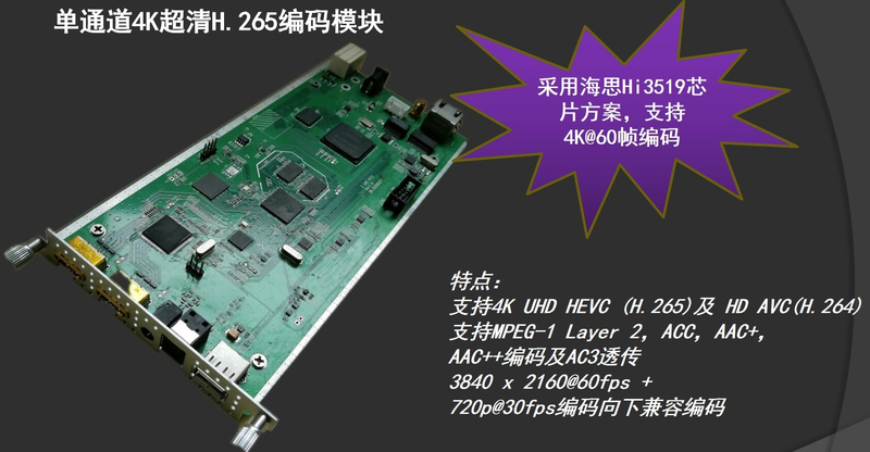 Single-Channel 4K Ultra-HD H.265 Encoder Module E-UD-0111-00-01
Communications & Energy
Prevail-catv
Input Interface - Type 1 [One Primary and One Backup]: HDMI*2 Input Interface - Type 2: Digital Audio (SPDIF) Input Interface - Type 3: Analog Audio
-
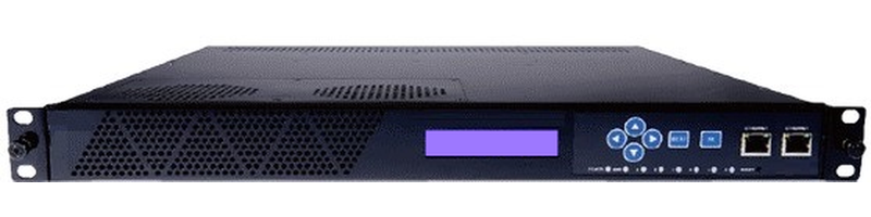 IP Switch WS-IP
Communications & Energy
Prevail-catv
WS-IP Professional Broadcast IP Switcher,Years of Development/Improvement,Excellent Performance,Meets Relevant National Standards.
-
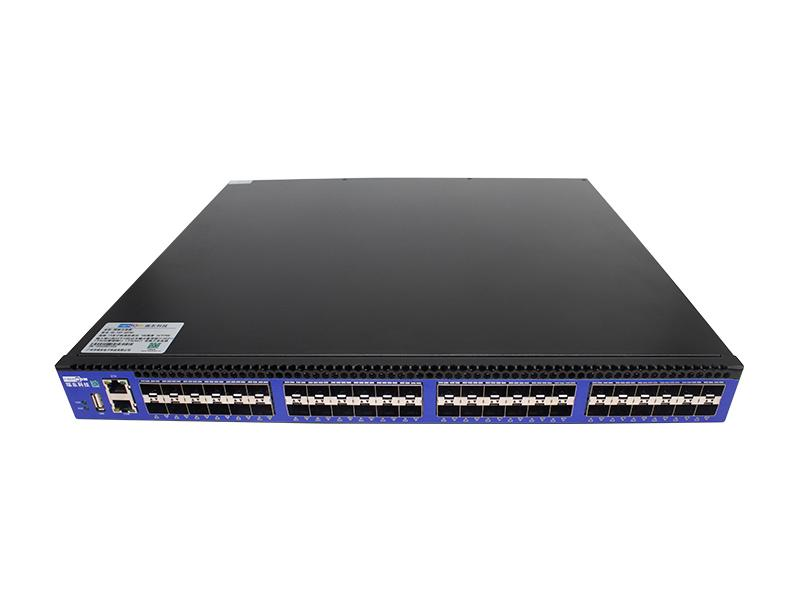 Enhanced SDH/POS Network Traffic Splitter / Network Traffic Replicator / Network TAP Switch RD-TAP-48P
Communications & Energy
Fiberwdm
Service Interface (POS): 24 Receivers for155M/622M/2.5G/10G POS and10G WAN;Each POS Rate Independently/Dynamically Switchable Service Interface (ETH): 24 10GE/1GE Transmit/Receive Channels Throughput (*) [Functions Listed Are a Collection; Functions and Interface Specifications Customizable by Scenario, Including but Not Limited to Those Listed]: 480Gbps
Enhanced SDH/POS Tap Converts to Ethernet,Flexible Efficient Collection/Filtering/Aggregation/Distribution/Load Balance/Replication for Traffic Control,Backup,Security.
-
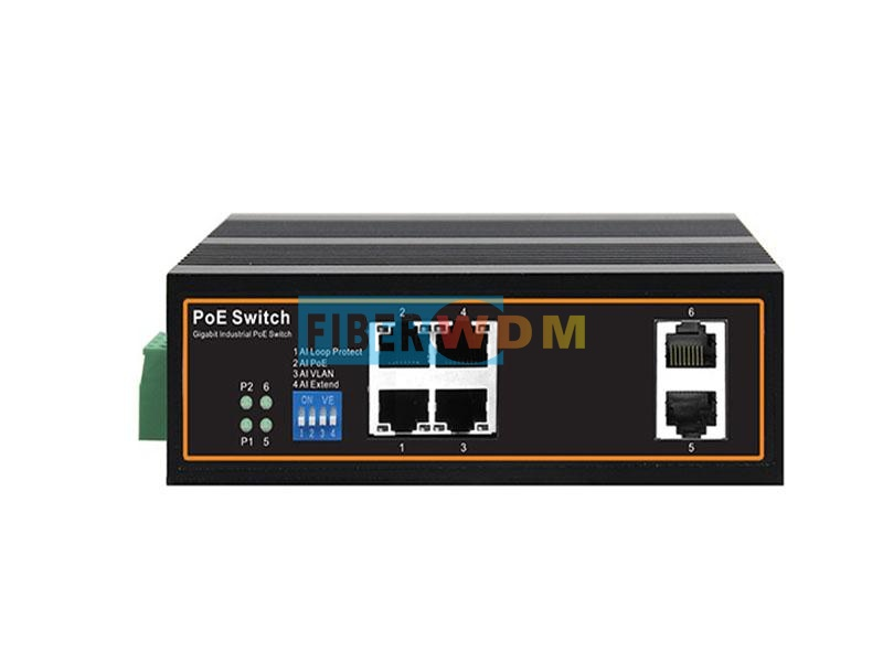 6-Electrical-Port POE Gigabit Industrial Switch FW304GPS-2G
Communications & Energy
Fiberwdm
Network Interface: 6 10/100/1000M RJ45 Ports Performance Specifications: MAC address table: 2k; backplane bandwidth: 12Gbps; packet forwarding rate: 8.9Mpps; forwarding mode: store-and-forward Power Supply Support: Maximum Output Power: 30W; Voltage Input: 48-56V DC; Input Method: Pluggable 5-Pin Terminal with 5.08mm Pitch
FW304GPS-2G is a quasi-industrial all-Gigabit managed PoE switch with six10/100/1000M adaptive RJ45 ports;the description also specifies two10/100/1000M RJ45 uplinks. All ports support6KV lightning protection,with supply overtemperature/overvoltage and surge-current protection. IEEE802.3x full-duplex and half-duplex backpressure flow control are supported. IEEE802.3af/at provides up to30W PoE per port. Reliable protection suits complex environments. Redundant48–56VDC dual inputs support dual-DC or the stated dual-DC/AC redundant supply arrangements.
-
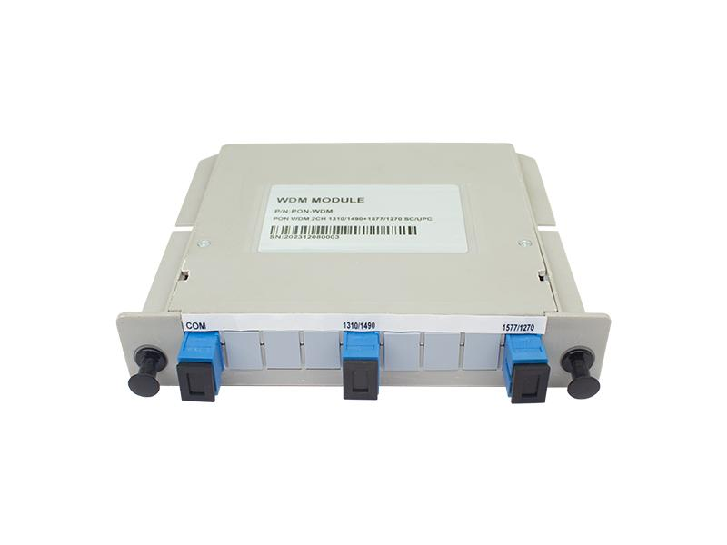 Broadband PON Network Single-Line Dual-Access Equipment FW-P801
Communications & Energy
Fiberwdm
Insertion Loss [Paired Single-Line Dual-Access Equipment; PDF Page 2 Product Features]: <1.6 dB
Single-Fiber Residential Drop Supports Multiple Broadband Services per User/Tenants or Fast Network Migration before Expiry,Avoids Second Entry Cable/Uses Existing Drop for Fast Installation.
Related Articles
VCSEL, short for Vertical Cavity Surface Emitting Laser, is a widely used semiconductor laser component in modern optoelectronics. Unlike traditional edge-emitting lasers, VCSEL emits laser light vertically from its chip surface. Thanks to its low power consumption, stable beam quality, low cost, and easy integration, it has become the core light source for 3D sensing, wearable devices, and high-speed optical communication.
As fundamental refractive optical components, plano‑convex spherical lenses consist of one convex spherical surface and one flat surface.
FiDAR, the fiber‑optic radar vehicle positioning and tracking system developed by Jianhe Bafang, is a high‑sensitivity distributed fiber‑sensing solution designed for intelligent traffic road monitoring. It outputs real‑time spatial coordinates of every vehicle across the full road section around‑the‑clock, delivering a brand‑new sensing technology for vehicle‑road cooperation, smart highway construction and urban traffic management.
Raybowlaser, a professional manufacturer of high-power laser chips, has officially launched its upgraded new-generation 1470nm high-performance laser chip. Achieving groundbreaking progress in rated output power and wall-plug efficiency (WPE), this innovative laser chip delivers superior and reliable core light source solutions for medical cosmetology, industrial processing, agricultural applications and scientific research equipment.
Loading...
Name
Phone
Organization
Use Case

Database Platform