

ZAPM-R4024C-14DV-Z1
The ZAPM-R4024C-14DV-Z1 performs color-temperature measurement, ambient-light sensing (ALS), and proximity detection. An internal state machine enables low-power operation between proximity and ALS measurements for very low average power consumption. Pin Configuration and Functions. Product Specifications. 1. Absolute Maximum Ratings:stresses beyond these ratings may permanently damage the device. They are stress ratings only and do not imply functional operation at these or any other conditions beyond the recommended operating conditions. Prolonged exposure may affect reliability. All voltage values are relative to VSS. Electrical Characteristics (VDD=3V, Ta=25℃). ALS+IR Characteristics (VDD=3V, Ta=25℃, PEN=1). Proximity Characteristics (VDD=3V, Ta=25℃, PEN=1).
 Save to Favorites
Overview
Specifications
| Parameter | Value |
|---|---|
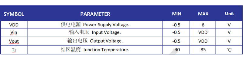
| Power-Supply Voltage VDD [Absolute Maximum Ratings;All Voltage Values Are Relative to VSS] | min :-0.5; max :6 |
| Voltage Input Input Voltage Vin [Absolute Maximum Ratings;All Voltage Values Are Relative to VSS] | min :-0.5; max :VDD |
| Output Voltage Vout [Absolute Maximum Ratings;All Voltage Values Are Relative to VSS] | min :-0.5; max :VDD |
| Junction Temperature Tj [Absolute Maximum Ratings;All Voltage Values Are Relative to VSS] | min :-40; max :85 |
| Human-Body Model (HBM) VESD [ESD Rating] | ±2000 V |
| Machine Model (MM) VESD [ESD Rating] | ±200 V |
| Power-Supply Voltage VDD [Recommended Operating Conditions] | min :2.5; typical :3.0; max :3.6 |
| Voltage Input Input Voltage Vin [Recommended Operating Conditions] | min :0; max :VDD |
| Output Voltage Vout [Recommended Operating Conditions] | min :0; max :VDD |
| Operating Ambient Temperature TA [Recommended Operating Conditions] | min :-20; max :70 |
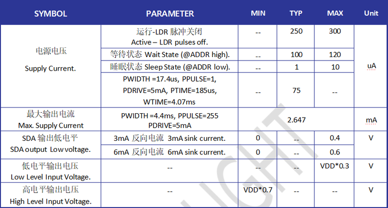
| Power Supply Voltage Supply Current [VDD=3V,Ta=25℃;Active - LDR Pulses Off] | typical :250; max :300 |
| Power Supply Voltage Supply Current [VDD=3V,Ta=25℃;Wait State (@ADDR High)] | typical :100; max :120 |
| Power Supply Voltage Supply Current [VDD=3V,Ta=25℃;Sleep State (@ADDR Low)] | typical :1; max :10 |
| Power Supply Voltage Supply Current [Electrical Characteristics ;VDD=3V,Ta=25℃;PWIDTH=17.4us;PPULSE=1;PDRIVE=5mA;PTIME=185us;WTIME=4.07ms] | typical :75 |
| Maximum Output Current Max. Supply Current [VDD=3V,Ta=25℃;PWIDTH=4.4ms;PPULSE=255;PDRIVE=5mA;Original Value Spans Minimum/Typical/Maximum Columns] | 2.647 mA |
| SDA Low Output Voltage [VDD=3V,Ta=25℃;3mA Reverse Current, English Label:3mA Sink Current] | min :0; max :0.4 |
| SDA Low Output Voltage [VDD=3V,Ta=25℃;6mA Reverse Current, English Label:6mA Sink Current] | min :0; max :0.6 |
| Low-Level Output Voltage (English Label:Low-Level Input Voltage) [Electrical Characteristics ;VDD=3V,Ta=25℃] | max :VDD*0.3 |
| High-Level Output Voltage (English Label:High-Level Input Voltage) [Electrical Characteristics ;VDD=3V,Ta=25℃] | min :VDD*0.7 |
| Output Low Level (SDA) VOL [Data-Transfer Timing Requirements;IOL=4mA] | max :0.5 |
| SCLK Operating Frequency fSCLK [Data-Transfer Timing Requirements] | max :400 |
| Stop and Start Conditions tBUF [Data-Transfer Timing Requirements] | min :1.3 |
| Hold Time after Repeated Start Conditions tHD;STA [Data-Transfer Timing Requirements] | min :0.6 |
| SCLK Clock Low Period tLOW [Data-Transfer Timing Requirements] | min :1.3 |
| SCLK Clock Low Period (English Label:SCLK Clock High Period) tHIGH [Data-Transfer Timing Requirements] | min :0.6 |
| Repeated-Start Condition Setup Time tSU;STA [Data-Transfer Timing Requirements] | min :0.6 |
| Count Hold Time (English Label:Data Hold Time) tHD;DAT [Data-Transfer Timing Requirements] | min :0; max :0.9 |
| Count Setup Time (English Label:Data Setup Time) tSU;DAT [Data-Transfer Timing Requirements] | min :100 |
| Clock/Count Fall Time (English Label:Clock/Data Fall Time) tF [Data-Transfer Timing Requirements] | max :300 |
| Clock/Count Rise Time (English Label:Clock/Data Rise Time) tR [Data-Transfer Timing Requirements] | max :300 |
| Stop-Condition Setup Time tSU;STO [Data-Transfer Timing Requirements] | min :0.6 |
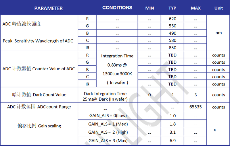
| ADC Peak-Wavelength Intensity (English Label:Peak Sensitivity Wavelength of ADC) [ALS+IR Characteristics ;VDD=3V,Ta=25℃,PEN=1; Channel =R] | typical :620 |
| ADC Peak-Wavelength Intensity (English Label:Peak Sensitivity Wavelength of ADC) [ALS+IR Characteristics ;VDD=3V,Ta=25℃,PEN=1; Channel =G] | typical :550 |
| ADC Peak-Wavelength Intensity (English Label:Peak Sensitivity Wavelength of ADC) [ALS+IR Characteristics ;VDD=3V,Ta=25℃,PEN=1; Channel =B] | typical :490 |
| ADC Peak-Wavelength Intensity (English Label:Peak Sensitivity Wavelength of ADC) [ALS+IR Characteristics ;VDD=3V,Ta=25℃,PEN=1; Channel =C] | typical :580 |
| ADC Peak-Wavelength Intensity (English Label:Peak Sensitivity Wavelength of ADC) [ALS+IR Characteristics ;VDD=3V,Ta=25℃,PEN=1; Channel =IR] | typical :850 |
| Dark Count Value [ALS+IR Characteristics ;VDD=3V,Ta=25℃,PEN=1;Dark Integration Time 25ms@Dark (In wafer)] | min :0; typical :1; max :3 |
| ADC Count Range [ALS+IR Characteristics ;VDD=3V,Ta=25℃,PEN=1] | max :65535 |
| Offset Ratio (English Label:Gain Scaling) [ALS+IR Characteristics ;VDD=3V,Ta=25℃,PEN=1;GAIN_ALS=0 (Low)] | typical :1.0 |
| Offset Ratio (English Label:Gain Scaling) [ALS+IR Characteristics ;VDD=3V,Ta=25℃,PEN=1;GAIN_ALS=1 (Med)] | typical :1.8 |
| Offset Ratio (English Label:Gain Scaling) [ALS+IR Characteristics ;VDD=3V,Ta=25℃,PEN=1;GAIN_ALS=2 (High)] | typical :3.1 |
| Offset Ratio (English Label:Gain Scaling) [ALS+IR Characteristics ;VDD=3V,Ta=25℃,PEN=1;GAIN_ALS=3 (Max)] | typical :6.9 |
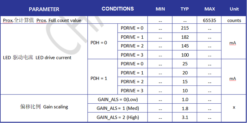
| Prox. Full Count Value [Proximity Characteristics ;VDD=3V,Ta=25℃,PEN=1] | max :65535 |
| LED drive current [Proximity Characteristics ;VDD=3V,Ta=25℃,PEN=1;PDH=0;PDRIVE=0] | typical :215 |
| LED drive current [Proximity Characteristics ;VDD=3V,Ta=25℃,PEN=1;PDH=0;PDRIVE=1] | typical :182 |
| LED drive current [Proximity Characteristics ;VDD=3V,Ta=25℃,PEN=1;PDH=0;PDRIVE=2] | typical :145 |
| LED drive current [Proximity Characteristics ;VDD=3V,Ta=25℃,PEN=1;PDH=0;PDRIVE=3] | typical :100 |
| LED drive current [Proximity Characteristics ;VDD=3V,Ta=25℃,PEN=1;PDH=1;PDRIVE=0] | typical :25 |
| LED drive current [Proximity Characteristics ;VDD=3V,Ta=25℃,PEN=1;PDH=1;PDRIVE=1] | typical :20 |
| LED drive current [Proximity Characteristics ;VDD=3V,Ta=25℃,PEN=1;PDH=1;PDRIVE=2] | typical :15 |
| LED drive current [Proximity Characteristics ;VDD=3V,Ta=25℃,PEN=1;PDH=1;PDRIVE=3] | typical :10 |
| Offset Ratio (English Label:Gain Scaling) [Proximity Characteristics ;VDD=3V,Ta=25℃,PEN=1;GAIN_ALS=0 (Low)] | typical :1.0 |
| Offset Ratio (English Label:Gain Scaling) [Proximity Characteristics ;VDD=3V,Ta=25℃,PEN=1;GAIN_ALS=1 (Med)] | typical :1.8 |
| Offset Ratio (English Label:Gain Scaling) [Proximity Characteristics ;VDD=3V,Ta=25℃,PEN=1;GAIN_ALS=2 (High)] | typical :3.1 |
| Loaded Quantity | 2000 pcs/reel |
Applications
Key Features
Datasheet
Supplier Information
Related Products
-
Single-Point Ranging Module PLM 14 Scanners and Rangefinders Lidar-tech
Ranging Accuracy [@15~59 (the source provides no separate unit at this segment)]: ±2 mm Ranging Accuracy [@60~120 (the source provides no separate unit at this segment)]: ±5 mm Ranging Accuracy [@121~200 (the source provides no separate unit at this segment)]: ±10 mm
Lingtu Technology's PLM14 single-point ranging module uses advanced single-photon detection and direct time of flight (dToF). It outputs digital serial data (IIC), with a measurement range of 15mm~200mm and near-range accuracy of ±2mm.
-
Single-Point Ranging Module PLM31 Scanners and Rangefinders Lidar-tech
Ranging Distance: Short range: 10≤x≤500mm; long range: 500<x≤6000mm Ranging Accuracy: Short range: ≤±10mm @10≤x<80mm, ≤±15mm @80≤x≤500mm, ≤±3mm @23mm; long range: ≤±15mm @500<x<1500mm, <±1% @1500≤x≤6000mm Ranging Frequency: Short range: 30Hz; long range: 120Hz
PLM31 is a single-point TOF edge-following ranging module with a measurement range of 10mm~6000mm. It flexibly switches between short- and long-range operating modes, with best short-range accuracy of ±3mm. Stable performance, a service life up to 10000 hours, very small size, flexible mounting and easy integration provide excellent cost-effectiveness; the source describes it as the best choice for cost reduction and efficiency improvement.
-
Single-Point Ranging Module PLM32 Scanners and Rangefinders Lidar-tech
Measurement Range [Reflectance: 1.0; interfering light intensity: <3kLux]: 0.03m~60m(反射率:1.0 ,干扰光强度:<3kLux) Precision and Accuracy [Reflectance: 1.0; interfering light intensity: <1kLux]: ±(1mm+D*(1/10000)) (reflectance: 1.0, interfering light intensity: <1kLux) Distance Resolution: 0. 1mm
0.5:610nm~690nm
-
 Barcode Scanning
Scanners and Rangefinders
Eldlaser
Semiconductor Barcode Scanning He's playing a very important role in modern society. 。 As technology continues to develop , Semiconductor Barcode Scanning Technology is widely used in all industries , Like retail. 、 Logistics 、 Manufacturing etc. 。 Its importance is reflected mainly in the following areas: : First of all , Semiconductor Barcode Scanning Technology can significantly improve efficiency 。 Scan through bar code , Staff have fast and accurate access to commodity information , Avoiding cumbersome manual entry. , Significant savings in time and human resources costs 。 In storage management , Barcode Scanning It helps managers locate the cargo quickly and accurately. , Increased efficiency of work , Reduced error rate 。 Second , Semiconductor Barcode Scanning Technology helps improve the accuracy and reliability of information 。 Scan through bar code , Human-induced input errors are avoided. , The accuracy of the information is ensured 。 In the area of logistics , Barcode Scanning Tracking and monitoring of goods , Ensuring the safe and timely delivery of goods 。 And... , Semiconductor Barcode Scanning Technology also improves client experience. 。 In the retail trade , Customers can access details by scanning the bar code of the goods. , To facilitate quick and easy understanding of product characteristics and prices , I've been able to get a better look at shopping. 。 Meanwhile... , Semiconductor Barcode Scanning You can also achieve the line below. None Sew Connection , Promotion of business development and innovation 。 Besides , Semiconductor Barcode Scanning Technology can also improve the management and competitiveness of enterprises 。 Pass. Barcode Scanning , Enterprises can achieve product inventories 、 Real-time monitoring and analysis of sales , Assisting enterprises in developing more accurate marketing strategies and supply chain management programmes , Improving the competitiveness and profitability of enterprises 。 In conclusion , Semiconductor Barcode Scanning The importance of the modern world is self-evident. 。 It's not only more efficient. 、 Information accuracy and customer experience , It also helps enterprises to upgrade their management and competitiveness. 。 As technology continues to develop , is. Semiconductor Barcode Scanning Technology will play an important role in more areas. , Promoting social progress and development 。
Related Articles
As a professional ultraviolet‑laser solution provider, Precilasers has launched its 266 nm narrow‑linewidth industrial laser, delivering reliable single‑frequency output for high‑precision interference lithography, semiconductor inspection and precision metrology applications.
On November 28, 2024, the 3rd China Laser Star Enterprise Summit & Advanced Laser Processing Technology Summit, an annual influential event in the laser industry, was grandly held in Wuhan Optics Valley.
Within cutting‑edge ultrafast photonics research, asynchronous optical sampling (ASOPS) and synchronous sampling serve as fundamental technologies for terahertz excitation detection, coherent Raman imaging and other time‑resolved spectroscopy experiments.
A laser bar is an array semiconductor laser chip integrated with dozens of emitters, which realizes hundred-watt quasi-continuous output on a single chip. With regular emitter arrangement and controllable fill factor, integrated thermal design and superior wall-plug efficiency compared to single chips, it acts as the core light source for high-power pumping, medical lasers and precision processing.
Loading...
Name
Phone
Organization
Use Case

Database Platform