


CVD Diamond
Diamond is a wide bandgap semiconductor material with excellent performance and has many advantages Extremely high thermal conductivity: thermal conductivity 2200W/mK, diamond has the highest thermal conductivity at room temperature ; extremely high dielectric breakdown characteristics: breakdown electric field is 107V/cm, 50 times that of GaAs, 2 times that of GaN, SiC 2.5 times ; extremely high power capacity: the allowable power capacity is more than 2500 times that of Si material; especially suitable for making high-power electronic devices; low dielectric constant: the dielectric constant is 5.7, about 1/2 of GaAs , which is less than half of InP ; high saturation carrier velocity: the saturation carrier velocity is 12.7 times that of GaAs, Si or InP, and maintains a high rate when the electric field strength increases ; high carrier mobility: electron mobility It is 4500c㎡/(V s), which is higher than most materials, and is suitable for making high-frequency electronic devices.
 Save to Favorites
Overview
Specifications
| Parameter | Value |
|---|---|
| Bulk Density | 3.3216 g/cm 3 |
| Thermal conductivity (W/(m*K)) | TC.1200;T.C1500;T.C1800 |
| Thermal diffusivity | 6.6; 8.2; 9.9 |
| Coefficient of thermal expansion (RT-700°C) (10 -6 K -1 ) | 3.1962 10 -6 K -1 |
| Moh's hardness | >10 |
| Tensile strength | 450~1100 Mpa |
| Young's modulus | 1000~1100 GPa |
| Dielectric constant (1MHz) | 5.68 |
| Dielectric loss (1MHz) | 6.2*10 -8 |
| Volume Resistivity [25°C] | 2.95 Ω cm × 1013 Ω cm |
| Insulation withstand voltage | DC 5.5KV/1.5mA |
| Transmittance | 40%~65% |
| Infrared absorption coefficient (cm -1 @1.064um) [@1.064um;cm -1 @1.064um;@1.064um)] | 0.3979~0.1871 cm -1 |
| Fine Polishing - Surface Roughness (Front) | Ra<1nm |
| Surface roughness (back side) | Ra<200nm |
| TTV [Ø25mm] | <1um(Ø25mm) |
| Warpage [Ø25mm] | <1um(Ø25mm) |
| Flatness PV [@633nm;Ø25mm;fringe@633nm;@633nm)] | 1.5fringe(Ø25mm) |
| Single Crystal Diamond-length*width | 10*10mm can be customized |
| Single Crystal Diamond-Length and Width Tolerance | ±0.05mm |
| Single Crystal Diamond-thickness | 0.2-2mm |
| Single Crystal Diamond-Thickness Tolerance | 0.1mm |
| Single Crystal Diamond-Crystal Orientation (Miscut) | ±3° |
| Single Crystal Diamond-crystallography | Usually 100% single sector {100} |
| Single Crystal Diamond-Horizontal dimension measurement | to the smaller side |
| Single Crystal Diamond-Edge features | <0.2mm |
| Single Crystal Diamond-edge orientation | Edge<100>&<110> |
| Single Crystal Diamond-facing towards | {110} |
| Single Crystal Diamond-edge laser cut | 3° |
| Single Crystal Diamond-1st and 2nd surface roughness | Polished, Ra<20nm |
| Single Crystal Diamond-Thermal expansion coefficient | 10( -6 )K −1 |
| Single Crystal Diamond-Thermal conductivity | 2200 W/(mk) |
| Single Crystal Diamond-nitrogen content | ① Ppb level: 20-50ppm; ② Ppm level: 20-30ppm |
Key Features
Datasheet
Please provide your email to download the datasheet.
Invalid email format. Please try again.
Supplier Information
Related Products
-
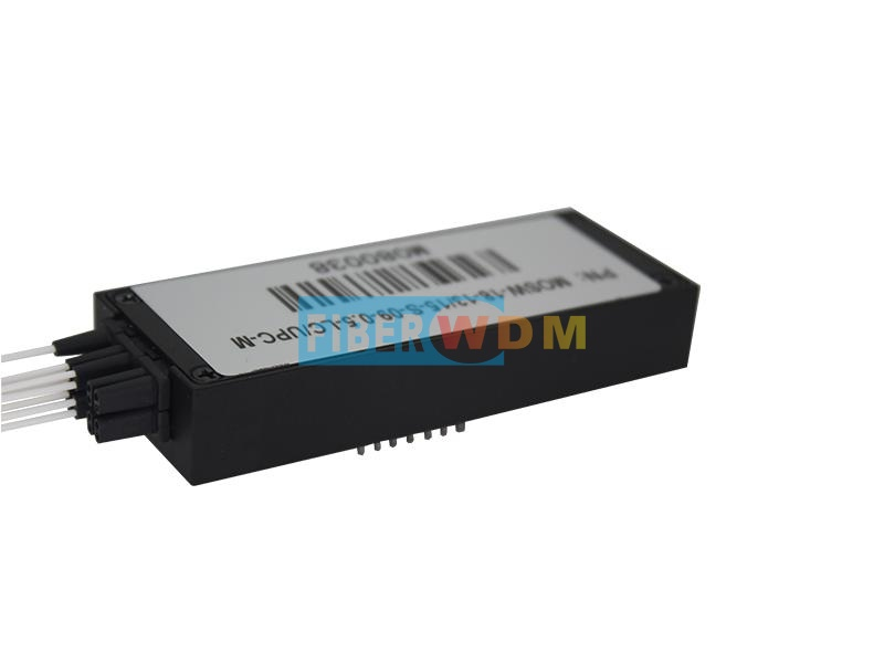 1XN MEMS Optical Switch
Semiconductor & Electronics
Fiberwdm
Wavelength [Or customer specify]: 13:1290~1330 15:1525~1568 16:1600-1650 Test Wavelength: 1310/1550/1625 or 1650 OSW Channels: 4/8/12/16/24/32/48/64
1xN MEMS Optical Switch 1xN MEMS optical switchis based on micro-electro-mechanical system technology. It allows channel selection between one input fiber and N output fibers by rotating the mirror of MEMS chip. The switch is bi-directional and can also be used as a Nx1 selector switch. The optical switch offers highly reliable, durable, long-life operation in a compact package.
-
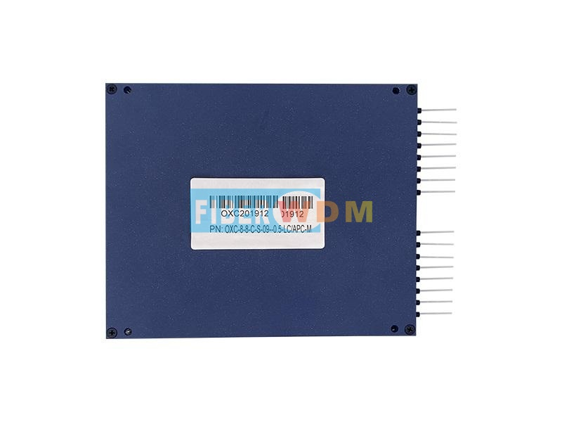 MXN MEMS Optical Switch
Semiconductor & Electronics
Fiberwdm
Wavelength [Or customer specify]: 1290~1330 1525~1568 1600-1650 Test Wavelength: 1310/1550/1625 or 1650 MxN [M*N≤1024]: 8x8/8x16/16x16/16x32
M x N MEMS Optical Switch OXC M x N MEMS Optical switch is used in optical cross-connect, OXC application. It’s also called Matric Optical Switch. It allows channel selections between M input fibers and N output fibers. FIBERWDM’s MEMS Modular Single-Mode OXC is based on industry proven, long-life, reliable MEMS 1xN optical switch components. Each MxN OXC consists of M 1xn OSW and N 1xm OSW.
-
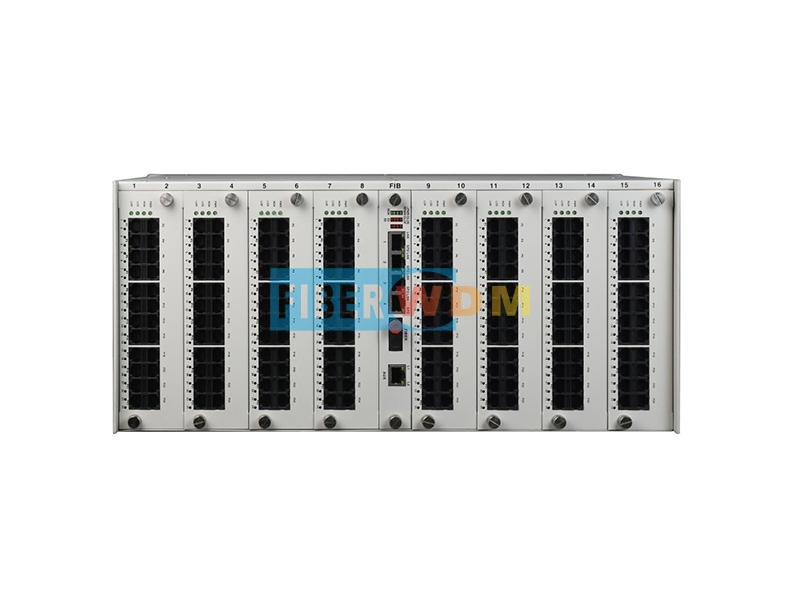 192-Channel Telephone Optical Transceiver FWOS192
Semiconductor & Electronics
Fiberwdm
Fiber Section - Optical Port: 1, 2 (1+1 Optical Backup) Fiber Section - Optical Port Rate: 3.125G Fiber Section - Optical Fiber: Single Fiber / Dual Fiber
广州瑞东 FWOS192 Point-to-Point ASIC Optical Terminal,4U19-Inch,192 RJ11 Phones/Eight Function Cards/One Dual-Optical Card,Complete Alarms,Stable/Reliable/Low Power/Integrated/Small.
-
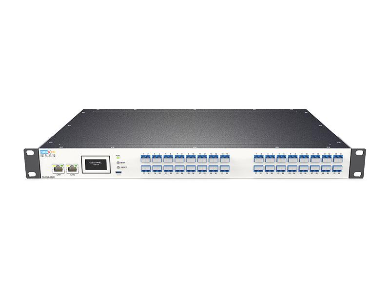 32×32 Fiber Switch, 1270-1610nm Single-Mode LC/UPC, 1U Rack FW-OSS-32X32
Semiconductor & Electronics
Fiberwdm
Total Number of Fiber Ports: 64 or Other Matrix Switching Scale: 32×32 Operating Wavelength Range: 1260~1660 Nanometers
FiberWDM (瑞东科技)'s FW-OSS-32X32 MEMS optical switch is a patented, high-performance, fully nonblocking all-optical matrix with configurable ports. Its 64 peer fiber ports allow arbitrary one-to-one connections. With no hardware-defined inputs/outputs, FiberWDM's GUI and embedded software configure any symmetric N×N or asymmetric N×M arrangement. Software-defined grouping partitions ports into any number of independently controlled groups, limited only by total port count. Software control and peer connectivity offer greater flexibility for optimized solutions. This versatile, easily deployed switch supports varied applications.
-
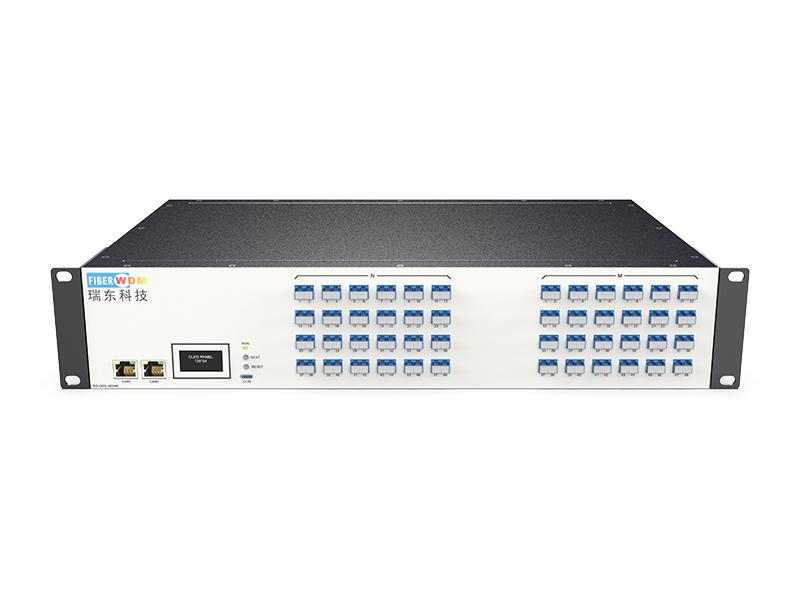 48×48 Fiber Switch, 1270-1610nm SM LC/UPC, 1U Rack FW-OSS-48X48
Semiconductor & Electronics
Fiberwdm
Total Number of Fiber Ports: 96 or Other Matrix Switch Dimensions: 48*48 Operating Wavelength Range: 1260 ~ 1660 nm
FiberWDM (瑞东科技)'s FW-OSS-48X48 MEMS optical switch is a patented, high-performance, fully nonblocking all-optical matrix with configurable ports. Its 96 peer fiber ports allow arbitrary one-to-one connections. With no hardware-defined inputs/outputs, FiberWDM's GUI and embedded software configure any symmetric N×N or asymmetric N×M arrangement. Software-defined grouping partitions ports into any number of independently controlled groups, each with any number of ports within the total-port limit. Software control and peer connectivity offer greater flexibility for optimized solutions. This versatile, easily deployed switch supports varied applications.
Related Articles
Developed by RealLight (Beijing), the R7M high‑power diode laser module belongs to the AW multi‑functional laser product family.
VCSEL, short for Vertical Cavity Surface Emitting Laser, is a widely used semiconductor laser component in modern optoelectronics. Unlike traditional edge-emitting lasers, VCSEL emits laser light vertically from its chip surface. Thanks to its low power consumption, stable beam quality, low cost, and easy integration, it has become the core light source for 3D sensing, wearable devices, and high-speed optical communication.
Fomoptic delivers integrated one‑stop optical solutions covering precision optical fabrication and custom vacuum coating services. Supported by complete processing production lines, comprehensive metrology equipment and experienced engineering team, we provide full‑chain customized components, ranging from blank shaping, ultra‑precision polishing to thin‑film coating, for laser systems, infrared imaging, industrial optics and scientific‑research projects.
For pulsed laser and full-spectrum optical testing, photodiodes and thermopiles have inherent drawbacks. Photodiodes show weak response in infrared band, while thermopiles feature slow response and cannot capture nanosecond narrow pulses.
Loading...
Name
Phone
Organization
Use Case

Database Platform