

Metalens Optical Inspection Systems MetronLens
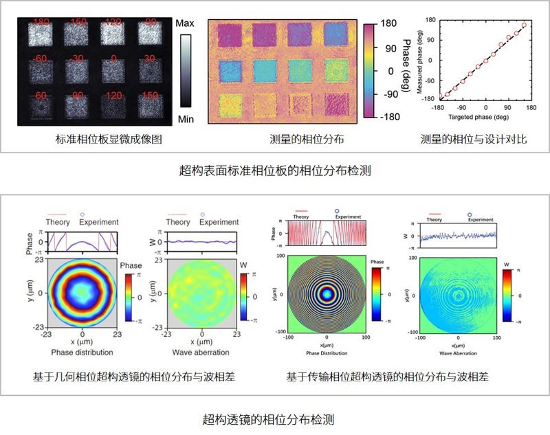
The MetronLens metalens optical inspection system is dedicated to planar optical components including metalenses, metasurfaces, and microlens arrays. It combines microscopic imaging, off-axis digital holography, far-field imaging, and other advanced technologies for in-situ inspection of optical-field, phase, and far-field distributions. It reveals the physical characteristics of planar optical components and provides a powerful tool for verifying design accuracy and optimizing fabrication processes.
 Save to Favorites
Overview
Specifications
| Parameter | Value |
|---|---|
| Measurement Mode | Transmitted optical-field distribution detection, transmitted far-field distribution detection |
| Measurable Optical Parameters | Optical-field distribution, focal length, numerical aperture, PSF, MTF, relative focusing efficiency, imaging resolution, far-field distribution |
| System Numerical Aperture [@ 40X] | 0.75 @ 40X |
| Field of View [@ 40X;@ 5X] | Φ0.5mm @ 40X,Φ4mm @ 5X |
| Spatial Resolution [@ 40X;@ 5X] | 0.45μm @ 40X,2.35μm @ 5X |
| z-Axis Scan Accuracy | ±1μm (0~1mm Travel ),±3μm (1~22mm Travel ) |
| Maximum Focal Length Measurement Range | 5mm |
| Standard Light Source | 532nm continuous-wave fiber laser |
| Incident Collimated Beam Divergence | 0.2° |
| Light Source Expansion Interface | 1 FC/APC Interface |
| Optional Module-Polarization Expansion | Supports incident / collection polarization elements, compatible with 4mm-thick polarizers |
Applications
Key Features
Datasheet
Supplier Information
Related Products
-
Tera3001-SA dual-LENS multidaughterboard coupling equipment Optical Lenses Terawan
The Tera3001-s multidaughterboard automatic alignment platform serves 10G/14G/25G optical transceivers. It mainly aligns lenses in Chip On Board (COB) modules, with single- or dual-channel lens/source alignment, automatic dispensing, and UV curing. The Tera3001-S provides high coupling efficiency, stability, and UPH depending on customer design, plus one-button collision protection and UV protection.
-
355 field lens Optical Lenses Central-laser
Focal Length [Original Table Row 2; Focal Length=100mm; Parallel Values in the Same Row Not Split into Separate Models or Configurations]: 100 mm Working Distance [Original Table Row 2; Focal Length=100mm; Parallel Values in the Same Row Not Split into Separate Models or Configurations]: 136 mm Scan Range [Original Table Row 2; Focal Length=100mm; Parallel Values in the Same Row Not Split into Separate Models or Configurations]: 70 mm² × 70 mm²
355 field lens: large zinc-selenide (ZnSe) focusing lens with a small spot for accurate marking. Imported lens material provides long service life and reduces removal, installation, and alignment. The 355nm scanning field lens is suitable for ultraviolet laser-marking machines.
-
532 field lens Optical Lenses Central-laser
Focal Length [Original Table Row 2; Focal Length=100mm; Parallel Values in the Same Row Not Split into Separate Models or Configurations]: 100 mm Working Distance [Original Table Row 2; Focal Length=100mm; Parallel Values in the Same Row Not Split into Separate Models or Configurations]: 114.5 mm Scan Range [Original Table Row 2; Focal Length=100mm; Parallel Values in the Same Row Not Split into Separate Models or Configurations]: 70 mm² × 70 mm²
532 field lens: large zinc-selenide (ZnSe) focusing lens with a small spot for accurate marking. Imported lens material provides long service life and reduces removal, installation, and alignment. The 532nm field lens is suitable for green laser-marking machines.
-
CO2 field lens Optical Lenses Central-laser
Focal Length [Original table row 2; Focal length=72mm; Parallel values in the same row, without additional model or configuration splitting]: 72 mm Mirror Diameter [Original table row 2; Focal length=72mm; Parallel values in the same row, without additional model or configuration splitting]: 48 mm Scan Range [Original table row 2; Focal length=72mm; Parallel values in the same row, without additional model or configuration splitting]: 50 mm² × 50 mm²
CO2 field lens: large zinc-selenide (ZnSe) focusing lens with a small spot for accurate marking. Imported lens material provides long service life and reduces removal, installation, and alignment. The 10640nm scanning field lens is suitable for CO2 laser-marking machines.
-
YAG field lens Optical Lenses Central-laser
Focal Length [Original table row 2; Focal length=63mm; Parallel values in the same row, without additional model or configuration splitting]: 63 mm Working Distance [Original table row 2; Focal length=63mm; Parallel values in the same row, without additional model or configuration splitting]: 78 mm Scan Range [Original table row 2; Focal length=63mm; Parallel values in the same row, without additional model or configuration splitting]: 50 mm² × 50 mm²
YAG field lens: large zinc-selenide (ZnSe) focusing lens with a small spot for accurate marking. Imported lens material provides long service life and reduces removal, installation, and alignment. The 1064nm scanning field lens is suitable for fiber laser-marking machines.
Related Articles
The LZFL405‑80mW‑3 series from Shenzhen Leirte Optoelectronics Co., Ltd. is a coaxial‑packaged violet‑blue single‑mode fiber‑coupled laser diode. It delivers 80 mW continuous‑wave output at 405 nm. Light is coupled into 3 μm core‑diameter single‑mode fiber for clean beam quality and easy integration into diverse optical systems. It serves as a compact violet‑blue light source for medical instruments and industrial printing applications.
Wuhan Optics Valley Quantum Technology Co., Ltd. is a leading domestic developer of high‑speed semiconductor optical chips and photodetector components. Our product portfolio covers InGaAs avalanche photodiode bare dies and PIN photodetector chips designed for fiber‑optic communication
As a professional ultraviolet‑laser solution provider, Precilasers has launched its 266 nm narrow‑linewidth industrial laser, delivering reliable single‑frequency output for high‑precision interference lithography, semiconductor inspection and precision metrology applications.
Electro-optic deflectors (EODs) are optical devices used to steer or deflect light beams by applying an electric field to a specialized optical crystal. Unlike mechanical beam steering systems that rely on moving mirrors, electro-optic deflectors enable high-speed, non-mechanical beam control with exceptional precision and responsiveness. They are widely used in laser scanning, optical communications, microscopy, laser printing, spectroscopy, and scientific research, where rapid and accurate laser beam positioning is essential.
Loading...
Name
Phone
Organization
Use Case

Database Platform