
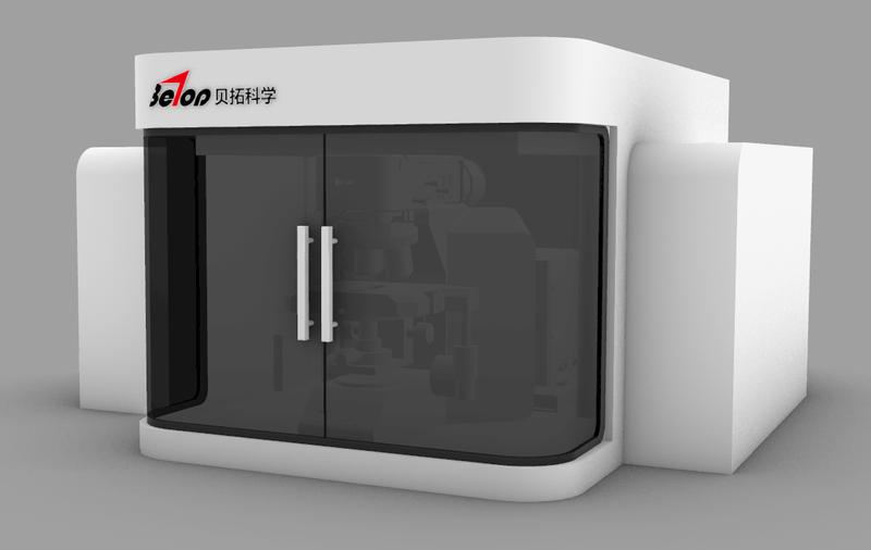

Specifications
| Parameter | Value |
|---|---|
| Laser | 532nm TEM00 Single-Mode Laser, 50mW |
| Laser | 638nm Single-Mode Laser, 50mW |
| Laser | 785nm Single-Mode Laser, 100mW |
| High-Sensitivity Spectrometer Focal Length | 300 mm |
| Spectrometer Spectral Range | Can Cover 200-1100nm |
| Grating | Three gratings with 600, 1200 and 1800 lines can be installed simultaneously; fully automatic software-controlled switching without manual grating replacement |
| Raman Spectral Range | Can Cover 100-5000cm-1 |
| White-Light Spectrum [Without Rotating the Grating] | Entire 530nm to 800nm spectrum acquired in one exposure without rotating the grating or stitching spectra by grating rotation |
| Spectral Resolution | Better Than 2 cm⁻¹ |
| Spectral Repeatability [Routine-lab test: single-crystal silicon; 532nm excitation; 100x objective; 100 repeats; repeatability of the 520cm⁻¹ silicon Raman-peak position] | Better Than 0.05 cm⁻¹ |
| High Sensitivity [Test: single-crystal silicon; 532nm laser, ≤10.0mW; 60s integration; 5 accumulations; 100x microscope objective] | The fourth-order silicon Raman peak is clearly observable. The third-order silicon Raman peak (about 1440cm⁻¹) has signal-to-noise ratio better than 20:1. No obvious N₂ or O₂ Raman peaks; their intensities must not exceed the fourth-order peak. |
| Spectral Detector | High-end back-illuminated CCD; peak quantum efficiency >=90%; TE cooling to -60 degrees |
| True Pinhole Confocal System | For optimum confocal performance, the system must use true pinhole confocal operation rather than slit-based pseudo-confocal operation. Pinhole diameter is automatically and continuously adjustable from 10 to 100um. |
| Lateral (XY) Optical Spatial Resolution [100× dry obj.; confocal hole≥50mm; auto stage. 1D nanomaterial Ø≤50nm (perfect graphene edge OK; no grating); Raman scan⊥material, 50nm steps; intensity-profile FWHM defines lateral Raman optical resolution.] | ≤ 500 nm @ 532 nm |
| Longitudinal (Z) Spatial Resolution [100× dry obj.; confocal aperture≥50mm. Suspended few-layer graphene; Raman Z scan in 50nm steps with 100X obj.; FWHM of G-peak intensity profile defines axial Raman-imaging optical resolution.] | ≤ 1000 nm@532 nm |
| Optical Microscope | The Optical Microscope Uses Köhler Illumination |
| Brightfield/Darkfield Objective | 10x Objective, 50x Objective (Long Working Distance), 100x Objective |
Datasheet
Please provide your email to download the datasheet.
Invalid email format. Please try again.
Supplier Information
Related Products
-
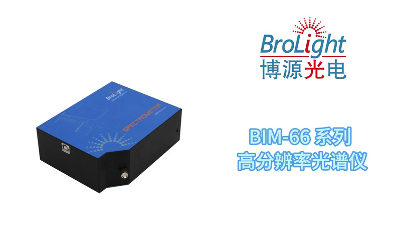 BIM-6602A series high-resolution spectrometers UV-NIR BIM-6602A-15
Spectrometers
Brolight
Fiber Connectors [BIM-6602A: Parameter Specifications]: SMA905 Detector [BIM-6602A: Parameter Specifications]: Hamamatsu S11639, Line-Array CMOS Detector Pixel [BIM-6602A: Parameter Specifications]: 2048 Pixels, Each Pixel 14μm×200μm
The BIM-6602A series spectrometer uses a high-resolution optomechanical structure in a compact, portable design, with resolution as fine as 0.08 nm. Interchangeable gratings adjust optical resolution and spectral range. Upgraded circuitry provides a 10000:1 dynamic range, minimum integration time of 0.5 milliseconds, and 600:1 signal-to-noise ratio for weak-signal detection. RS232 communication and improved interference resistance make it ideal for industrial and scientific applications.
-
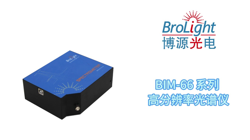 BIM-6602A series high-resolution spectrometers UV-NIR BIM-6602A-16
Spectrometers
Brolight
Fiber Connectors [BIM-6602A: Parameter Specifications]: SMA905 Detector [BIM-6602A: Parameter Specifications]: Hamamatsu S11639, Line-Array CMOS Detector Pixel [BIM-6602A: Parameter Specifications]: 2048 Pixels, Each Pixel 14μm×200μm
The BIM-6602A series spectrometer uses a high-resolution optomechanical structure in a compact, portable design, with resolution as fine as 0.08 nm. Interchangeable gratings adjust optical resolution and spectral range. Upgraded circuitry provides a 10000:1 dynamic range, minimum integration time of 0.5 milliseconds, and 600:1 signal-to-noise ratio for weak-signal detection. RS232 communication and improved interference resistance make it ideal for industrial and scientific applications.
-
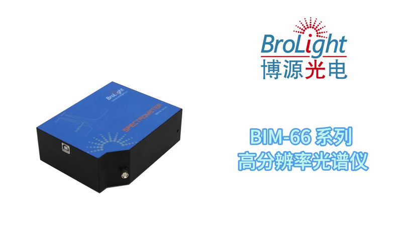 BIM-6602A series high-resolution spectrometers UV-NIR BIM-6602A-17
Spectrometers
Brolight
Fiber Connectors [BIM-6602A: Parameter Specifications]: SMA905 Detector [BIM-6602A: Parameter Specifications]: Hamamatsu S11639, Line-Array CMOS Detector Pixel [BIM-6602A: Parameter Specifications]: 2048 Pixels, Each Pixel 14μm×200μm
The BIM-6602A series spectrometer uses a high-resolution optomechanical structure in a compact, portable design, with resolution as fine as 0.08 nm. Interchangeable gratings adjust optical resolution and spectral range. Upgraded circuitry provides a 10000:1 dynamic range, minimum integration time of 0.5 milliseconds, and 600:1 signal-to-noise ratio for weak-signal detection. RS232 communication and improved interference resistance make it ideal for industrial and scientific applications.
-
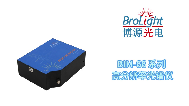 BIM-6602A series high-resolution spectrometers UV-NIR BIM-6602A-18
Spectrometers
Brolight
Fiber Connectors [BIM-6602A: Parameter Specifications]: SMA905 Detector [BIM-6602A: Parameter Specifications]: Hamamatsu S11639, Line-Array CMOS Detector Pixel [BIM-6602A: Parameter Specifications]: 2048 Pixels, Each Pixel 14μm×200μm
The BIM-6602A series spectrometer uses a high-resolution optomechanical structure in a compact, portable design, with resolution as fine as 0.08 nm. Interchangeable gratings adjust optical resolution and spectral range. Upgraded circuitry provides a 10000:1 dynamic range, minimum integration time of 0.5 milliseconds, and 600:1 signal-to-noise ratio for weak-signal detection. RS232 communication and improved interference resistance make it ideal for industrial and scientific applications.
-
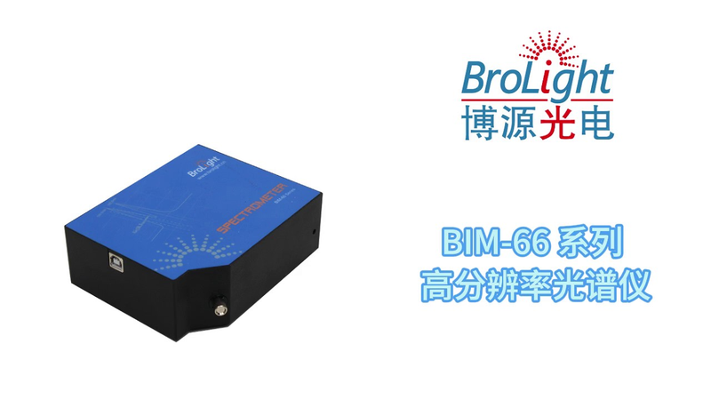 BIM-6602A series high-resolution spectrometers UV-NIR BIM-6602A-19
Spectrometers
Brolight
Fiber Connectors [BIM-6602A: Parameter Specifications]: SMA905 Detector [BIM-6602A: Parameter Specifications]: Hamamatsu S11639, Line-Array CMOS Detector Pixel [BIM-6602A: Parameter Specifications]: 2048 Pixels, Each Pixel 14μm×200μm
The BIM-6602A series spectrometer uses a high-resolution optomechanical structure in a compact, portable design, with resolution as fine as 0.08 nm. Interchangeable gratings adjust optical resolution and spectral range. Upgraded circuitry provides a 10000:1 dynamic range, minimum integration time of 0.5 milliseconds, and 600:1 signal-to-noise ratio for weak-signal detection. RS232 communication and improved interference resistance make it ideal for industrial and scientific applications.
Related Articles
The ElFys PD25s series photodetectors adopt ElFys‑patented Black Silicon Induced Junction technology, delivering excellent spectral response spanning deep‑ultraviolet, visible and near‑infrared bands for diverse high‑precision photometry applications. Sub‑variants including H, M, HG and MG are optimised for low‑capacitance, low‑dark‑current and high‑reverse‑bias guard‑ring operations respectively. Multiple packaging configurations are available to satisfy various system‑design requirements.
Fomoptic delivers integrated one‑stop optical solutions covering precision optical fabrication and custom vacuum coating services. Supported by complete processing production lines, comprehensive metrology equipment and experienced engineering team, we provide full‑chain customized components, ranging from blank shaping, ultra‑precision polishing to thin‑film coating, for laser systems, infrared imaging, industrial optics and scientific‑research projects.
Wuhan Optical Valley Interlink Technology Co., Ltd. was founded in 2013 by a technical team from Huazhong University of Science and Technology.
For semiconductor, coating and laboratory vacuum chambers, thermal conductivity gauges suffer large measurement errors caused by gas type and ambient temperature.
Loading...
Name
Phone
Organization
Use Case

Database Platform