

SPP Teaching instrument
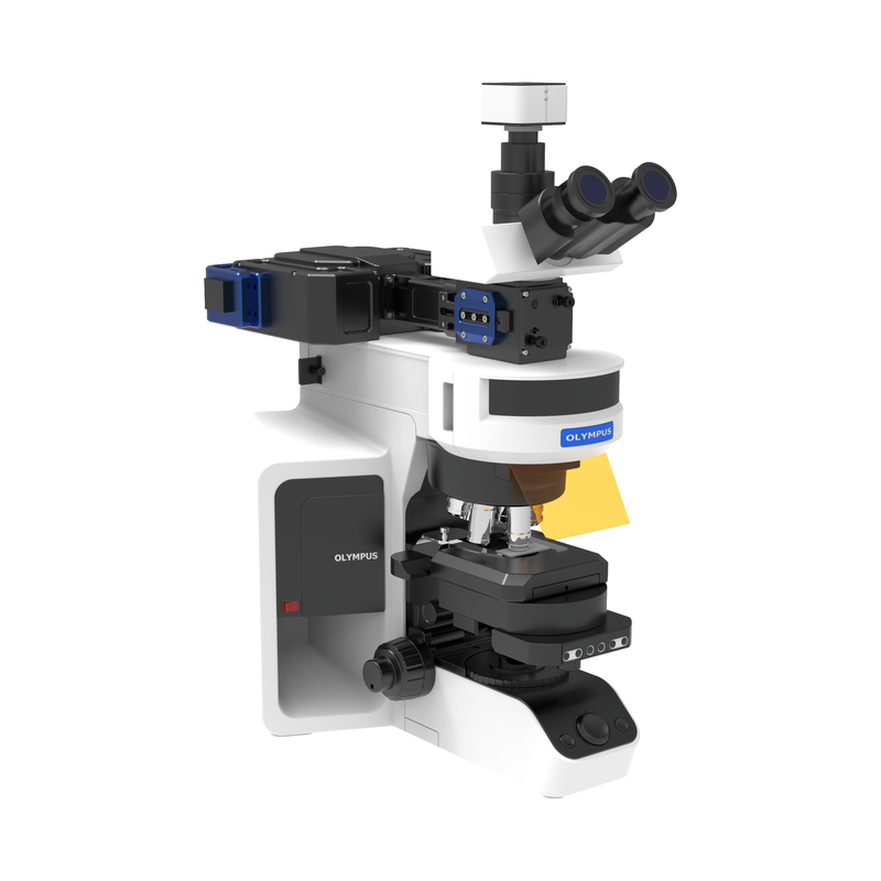
This SPP teaching instrument supports courses in modern optics, thin-film optics, nanophotonics, microscopy and optical sensing. A one-dimensional photonic crystal controls the incident angular spectrum and polarization so that momentum-matched TM components excite surface plasmon polaritons (SPPs) at a gold-film/dielectric interface. Particles scatter the interfacial near field for microscopy and dynamic sensing. Independently adjustable illumination, coupling, sample, imaging and acquisition modules support fundamental demonstrations and integrated experiments. In the transmitted field of the one-dimensional photonic crystal, momentum-matched transverse-magnetic components couple to SPPs at the gold-film interface. These electromagnetic surface modes propagate along the metal-dielectric boundary and decay exponentially perpendicular to it. The modular optical chain comprises a low-coherence LED, scattering layer, one-dimensional photonic crystal, gold-film/SPP interface, microscope objective, tube lens and scientific camera. Multiple random scattering of red LED illumination produces a broad angular distribution and multiple polarization components for momentum-space filtering. Compared with coherent laser illumination, the low-coherence LED reduces speckle and interference artifacts for a more uniform, stable image background. Particles on the gold film or within the effective near field perturb the local field according to their refractive index, size, shape or surface state, scattering surface-mode energy into far-field light. Scattering intensity and its temporal changes characterize size, aggregation, hygroscopic behavior, chemical reactions and local refractive-index changes for micro/nanoparticle imaging, quantitative detection and dynamic sensing. The system compares ordinary dark-field and SPP-enhanced scattering imaging. Five progressive experimental modules cover core plasmonic photonics for advanced undergraduate and graduate teaching. First, build the on-chip SPP microscope and understand the scattering layer, photonic crystal, gold interface and imaging module. Establish a low-magnification baseline, focus and field center; install the scattering-layer–1DPC–gold-film structure; adjust sample height and lateral position; select target and background ROIs and calculate mean intensity, standard deviation, SBR and SNR; and compare blank backgrounds, standard particles and missing-layer controls for stability. Second, investigate high-angle TM coupling and observe particles on or near the film to verify SPP-enhanced scattering. Apply polarization and momentum-matching conditions; record bright-spot counts and integrated intensity over several fields at low particle concentration; vary polarization, wavelength or chip orientation; and use blank and gold-free substrates to isolate the enhancement. Third, calibrate scattering intensity against standard particle size, considering Rayleigh scattering and background-interference effects on scaling. Analyze at least 20 isolated particles per size using identical ROIs and background-subtracted integrated intensity, plot intensity against diameter, estimate the scaling exponent by linear regression, and discuss saturation, overlap and selection bias. Fourth, vary relative humidity to change particle size or refractive index and obtain sensing curves. Establish a low-humidity baseline, raise RH in steps with stabilization, then lower it to examine hysteresis. Register the same particles, normalize responses and plot intensity against RH to assess transition points, repeatability and hysteresis. Fifth, track intensity, color or morphology to study nanomaterial reaction, dissolution, aggregation, adsorption and interfacial transitions. Monitor scattering in real time, observe dynamic behavior, extract kinetic parameters from time series and explore new optical characterization methods. Course objectives are: 1. Explain the angular selectivity of one-dimensional photonic crystals and their control of high-wavevector TM components for SPP coupling. 2. Analyze TE/TM transmission with transfer matrices or experiments. 3. Understand momentum matching, near-field interaction and enhanced particle scattering. 4. Independently align optics, acquire images, perform quantitative analysis and discuss uncertainty. 5. Write a course-paper-style report with abstract, methods, results, discussion and references.
 Save to Favorites
Overview
Applications
Key Features
Datasheet
Please provide your email to download the datasheet.
Invalid email format. Please try again.
Supplier Information
Related Products
-
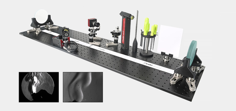 OEDU-GSME Schlieren Experiment Demonstration Kit
Research & Education
Oeabt
Using the knife-edge method, the system converts light-ray deflection into intensity changes. Lower-density regions, such as hot airflow, deflect rays in a particular direction and form brighter spots at the knife edge; higher-density regions form darker spots. The camera thus records an image representing the density distribution.
-
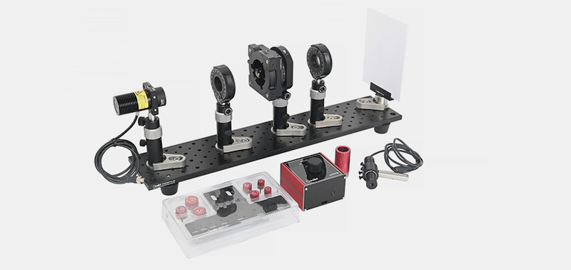 OEDU-PLE Light Polarization Experiment
Research & Education
Oeabt
Light polarization experiments investigate polarization properties and behavior in different media and optical devices, demonstrating polarization phenomena and their applications in science and technology.
-
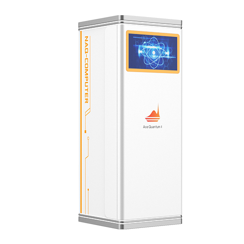 Neutral-Atom Quantum Computing System and Submodules
Research & Education
Acephoton
The company has developed a neutral-atom quantum computing system and submodules to provide a full-stack quantum computing solution from core devices to complete-system architecture. Based on advanced neutral-atom technology, it integrates atom trapping, optical-tweezer arrays, quantum-state manipulation and readout. A flexible modular architecture allows core submodules to run independently for individual technology verification or connect seamlessly for coordinated operation, simplifying assembly, upgrades and maintenance. Serving university research, algorithm development and commercialization exploration, these highly stable, scalable system-level products lower R&D barriers and accelerate deployment and scale-up of neutral-atom quantum computing.
-
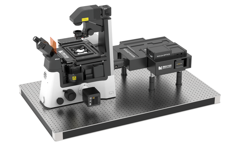 Holographic Optical Tweezers Configuration Parameters
Research & Education
Kayjaopt
Configuration Parameters-Holographic Optical Tweezers Module: 1) Generates ≥100 optical traps simultaneously for particles of 1-50μm. 2) Spatial phase modulation 0-2π, response band 1000-1100nm, light utilization ≥97% (@1064nm), 1272*1024 pixels, pixel size 12.5μm and effective area 15.9mm*12.8mm; select the SLM response band to match the laser wavelength. 3) Dynamically adjustable trapping force. 4) Supports Fresnel, cylindrical and conical lenses, gratings, Laguerre-Gaussian beams, combinations and custom 3D manipulation. 5) A 1064nm laser, with other wavelengths optional, power ≥3W, beam quality M2 of 1.2, modulation frequency 10khz and a laser cooling module. 6) Force measurement accuracy 0.5pN. Configuration Parameters-Single-Trap Independent Control Module: 1) Includes a single high-power 1W 1064nm laser, with other wavelengths optional. A galvanometer scanner enables high-speed two-dimensional movement of a single optical trap, complementing the SLM in high-speed applications. Supports independent planar path planning and strong single-point trapping. 2) Includes a data acquisition card. Configuration Parameters-Microscope Main Body: 1) Nikon Ti2-U inverted microscope as standard; adapters and optical-path interfaces can also suit an existing laboratory microscope. 2) A 100X oil-immersion objective or 60X water-immersion objective dedicated to optical tweezers.
Holographic optical tweezers use mechanical light-matter interactions for precise three-dimensional microscopic manipulation and force analysis. A suitably distributed beam generates piconewton forces that trap and move viruses, bacteria, organelles, cells, micro/nanoscale transparent or metallic particles and micro/nanomotors without mechanical damage. Light penetration also enables manipulation of internal components without damaging particle surfaces. Noncontact operation, low damage, diverse targets and precise displacement/force measurement have led to use in life sciences, physical chemistry and aerosol science, with potential in micro/nanofabrication and sensing. Optical tweezers are essential for biophysical/biomechanical characterization; inventor ASHKIN received the 2018 Nobel Prize in Physics for their biological success. Near-infrared wavelengths, commonly 1064nm, are essentially nondestructive to biological specimens. Forces range from femtonewtons (10⁻¹⁵N) to hundreds of piconewtons (10⁻¹⁰N), matching microscopic biological forces. HoloGraphic Optical Tweezers (HOT) revolutionized optical trapping. Kaijia Photonics' SLM-HOT uses a liquid-crystal phase-only spatial light modulator (SLM; Spatial Light Molator) as a holographic element. Wavefront phase shaping generates trap arrays. Computer-loaded and switched holograms position traps; preset patterns simultaneously trap and manipulate multiple particles in 3D, with independent dynamic control of any array particle. New trap types rotate, transport and sort particles. Phase modulation can be added to one or more traps to generate special focal fields such as Bessel and vortex beams. K-Well commercial operating software sets laser power and camera parameters, generates/manipulates traps and arrays, plans straight/circular/rectangular/custom paths, provides multiple force-measurement methods, real-time mechanical analysis/display and holographic phase projection. K-BeamGenerator, developed for the company's tweezers, generates phase holograms for different SLM configurations. Modules: beam shaping with Laguerre, Airy and Hermite beams; diffractive optics including cosine/blazed gratings, axicons, cylindrical and Fresnel lenses; 3D point arrays with multiple positions and corresponding phase maps; custom grating/beam and grating/lens combinations.
-
 Laser-Scanning Optical Manipulation System
Research & Education
Kayjaopt
Controls focused-laser 2D scanning under a microscope with programmable scan paths. Galvanometer elements scan incident lasers from visible to near-infrared wavelengths in two dimensions, providing temporal scanning of specified spatial light-field structures. Suitable for single-photon and two-photon absorption experiments.
Related Articles
Macro channel water-cooled stacked laser diodes integrate dozens of laser bars into one vertical stacked module with large-diameter macro flow cooling channels.
Fomoptic delivers integrated one‑stop optical solutions covering precision optical fabrication and custom vacuum coating services. Supported by complete processing production lines, comprehensive metrology equipment and experienced engineering team, we provide full‑chain customized components, ranging from blank shaping, ultra‑precision polishing to thin‑film coating, for laser systems, infrared imaging, industrial optics and scientific‑research projects.
The accelerated construction of new‑generation power systems has brought revolutionary upgrades to power‑equipment maintenance workflows.
The MSL‑T series water‑cooled continuous‑wave single‑longitudinal‑mode lasers from Changchun New Industries Optoelectronics (CNI) deliver key research wavelengths including 369 nm, 405 nm and 770 nm.
Loading...
Name
Phone
Organization
Use Case

Database Platform