

Yb:YLF
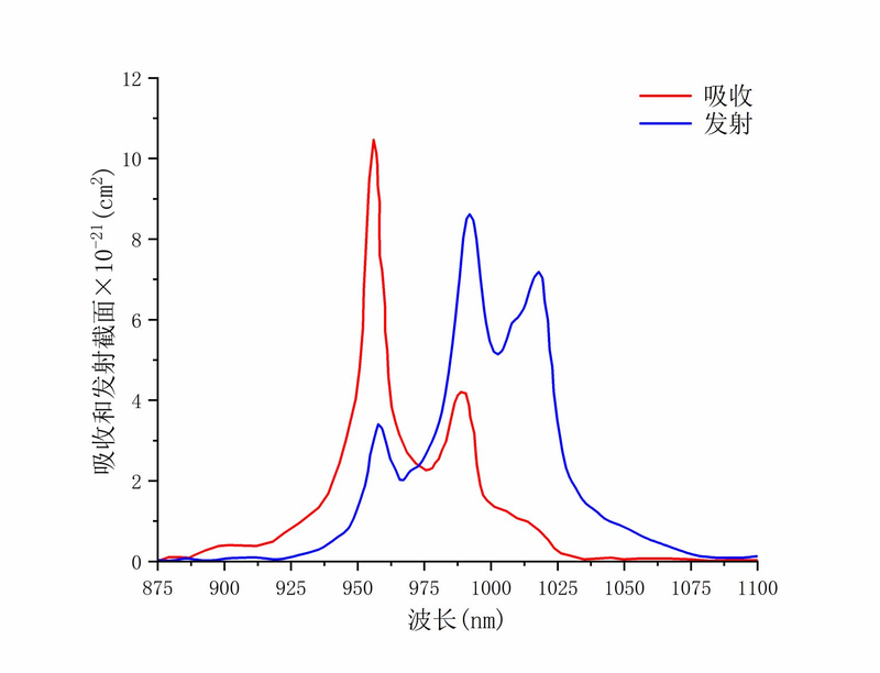
Yb:YLF is a laser crystal with excellent overall performance, widely used in laser cooling, cryogenic temperature measurement, and diode pumping. It features low quantum defect, high thermal conductivity, and a broad tuning range. Applications include mode-locked lasers, subpicosecond pulsed lasers, diode-pumped chirped-pulse regenerative amplifiers, and thin-disk lasers.
 Save to Favorites
Overview
Specifications
| Parameter | Value |
|---|---|
| Absorption peak wavelength | 960 nm |
| Peak Absorption bandwidth | ~10 nm |
| Laser Wavelength | 1017 nm |
| ²F₅/₂ Energy-level lifetime | 2.1ms |
| Refractive Index [@1040 nm] | ~1.4 |
| Crystal Structure | Tetragonal |
| Density | 3.95g/cm³ |
| Mohs Hardness | 5 |
| Thermal conductivity | 6 Wm⁻¹K⁻¹ |
| Coefficient of thermal expansion | 8×10⁻⁶(∥c)k⁻¹, 13×10⁻⁶(∥a)k⁻¹ |
| Typical doping level | 5%-20% |
| Orientation | a-cut |
| Clear Aperture Dimension | >90% |
| Face dimension tolerance | +0/-0.1mm |
| Length Tolerance | ±0.1mm |
| Parallelism error | <10 arcsec |
| Perpendicularity error | <10 arcmin |
| Protective groove [@45˚] | <0,1 mm @45˚ |
| Surface Quality | 10-5 S-D |
| Surface Flatness [@6328 nm] | <λ/10@6328 nm |
| Coating [@960 nm + AR(R<0.15%) @1000~1060 nm] | AR(R<0.5%) @960 nm + AR(R<0.15%) @1000~1060 nm |
| Laser Damage threshold [@1030 nm,10 ns] | >10 J/cm²@1030 nm,10 ns |
Key Features
Datasheet
Supplier Information
Related Products
-
 Er:Yb:Glass+Co:spinel
Laser Crystals
Xkpho
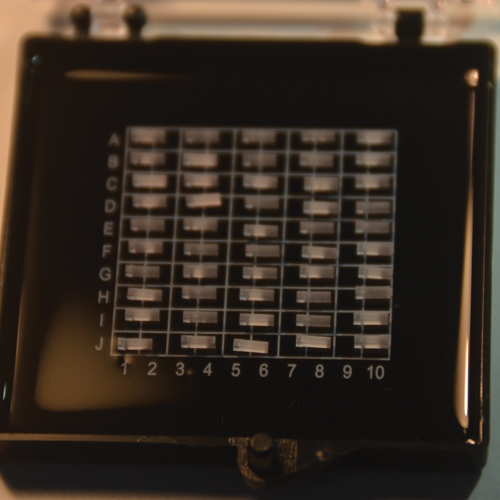
Material: Er:Yb:Glass+Co:MgAl2O4 Dimension: 0.9 mm × 0.9 mm × 3.7 mm Pumping: 915-955nm
-
 Nd:YVO4
Laser Crystals
Xkpho
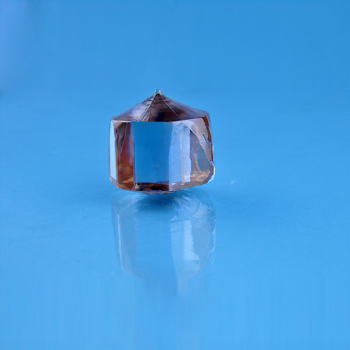
Atomic Density [Nd1.0%]: 1.26x10²⁰ atoms/cm3 (Nd1.0%) Crystal Structure: Zircon Tetragonal, space group D4h-I4/amd a=b=7.1193A,c=6.2892A Density: 4.22g/cm3
Nd:YVO4 is one of the most promising commercially available diode pumped solid state laser materials. It has high laser induced damage threshold and good mechanical in addition to optical properties. Its large stimulated emission cross-section and high absorption of pump laser make it a right crystal for pocket laser. Nd: YVO4 can produce IR green and blue laser by using minor different set-up. A broad absorption band centered at 808nm and favorable mechanical properties make Nd:YVO4 well suited for compact, efficient, high power diode-pumped lasers. Natural birefringence gives rise to a highly polarized output at 1064.3 and 1342nm.
-
 Titanium Sapphire Tunable Laser LX329
Laser Crystals
Antelaser
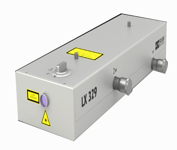
Maximum Pumping Energy: 110 mJ Repetition Rate: 10-30 Hz Harmonizing Range , nm / Base frequency: 700…980
-
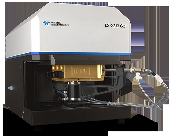 LSX-213 G2+ Nd:YAG Laser Ablation System
Laser Crystals
Hl-instruments
Laser Source: Five times. 213nm Q-switched Control Nd:YAG Solid Laser Source Laser Energy: >4mJ/pluse Pulse Width: <5ns
LSX-213 G2+ Optimized optical design using state-of-the-art technology 。 Use leather for durable use 、 And many harsh tests. LSX-G2 Platform , Provide super-stabilized optical performance and job stability 。 Provide all performance indicators required for routine analysis , Low operating cost , Easy to maintain 。 LSX-213 G2+ It's a closed-in. Pumping Lights and MIL One. SPEC Standard Designed and made. Laser Source , It's a super-stabilized operation. Laser Energy and minimal maintenance costs 。 It's ready. High Precision After the independent seismic optical platform ,LSX-213 G2+ Multiple sample analysis in multiple demanding environments 。 LSX-213 G2+ High performance hardware and high performance hardware with the latest technology High Precision Optical component design manufacture , It provides excellent optical resolution. , Achieving clear observations with a broad vision 。 Quality equipped 、 Multi-array and Brightness Adjustable Transmitting and reflecting lighting systems , Make sure you can also see the samples clearly at a very large multiplication. 。 LSX-213 G2+ A concise and practical structural design , Not only provide stable performance , It's also very easy to maintain. 。 Designed using open sample pool location , It's a multi-species pool. , and support users Custom Sample pool 。 Software Control Internal Aperture Auto Switch , Ripping the dot diameter range 4μm One. 200μm; System realization and ICP Two-way communications , Real time energy adjustment 、 Parameters such as dot size and scan speed ;CETAC The product facilitates your efficient work process , Achieving a fixed point —— Erosion —— Three step objectives of analysis 。
-
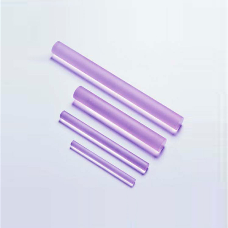 Titanium Doped Sapphire
Laser Crystals
Rsgx
Ti203 Concentration: 0.06~0.5wt% Figure of Merit: 100~300 mm Dimension: 2~50 mm
Related Articles
As a professional ultraviolet‑laser solution provider, Precilasers has launched its 266 nm narrow‑linewidth industrial laser, delivering reliable single‑frequency output for high‑precision interference lithography, semiconductor inspection and precision metrology applications.
On November 28, 2024, the 3rd China Laser Star Enterprise Summit & Advanced Laser Processing Technology Summit, an annual influential event in the laser industry, was grandly held in Wuhan Optics Valley.
Within cutting‑edge ultrafast photonics research, asynchronous optical sampling (ASOPS) and synchronous sampling serve as fundamental technologies for terahertz excitation detection, coherent Raman imaging and other time‑resolved spectroscopy experiments.
A laser bar is an array semiconductor laser chip integrated with dozens of emitters, which realizes hundred-watt quasi-continuous output on a single chip. With regular emitter arrangement and controllable fill factor, integrated thermal design and superior wall-plug efficiency compared to single chips, it acts as the core light source for high-power pumping, medical lasers and precision processing.
Loading...
Name
Phone
Organization
Use Case

Database Platform