
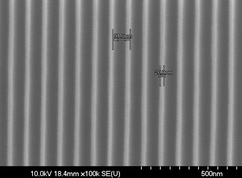
Large-Area Roller-to-Plate Nanoimprint Equipment
1. Imprint area: 1020mm*1520mm. 2. Imprint precision: minimum line width ≤30nm. 3. Imprint speed: ≥1m/min. 4. Roller pressure: dead weight + set rated pressure. 5. Fully automatic imprinting, exposure and demolding, with adjustable demolding angle. 6. UV source: 365nm LED, maximum rated power 500mw/cm^2; area-source size 1100mm*75mm. Exposure is completed by moving the source at constant speed. 7. The chamber includes an FFU and an antistatic device to maintain a good internal environment. 8. Graphical software interface with real-time production-data feedback.
 Save to Favorites
Overview
Specifications
| Parameter | Value |
|---|---|
| Imprinted Line Width | 20nm |
Datasheet
Please provide your email to download the datasheet.
Invalid email format. Please try again.
Supplier Information
Related Products
-
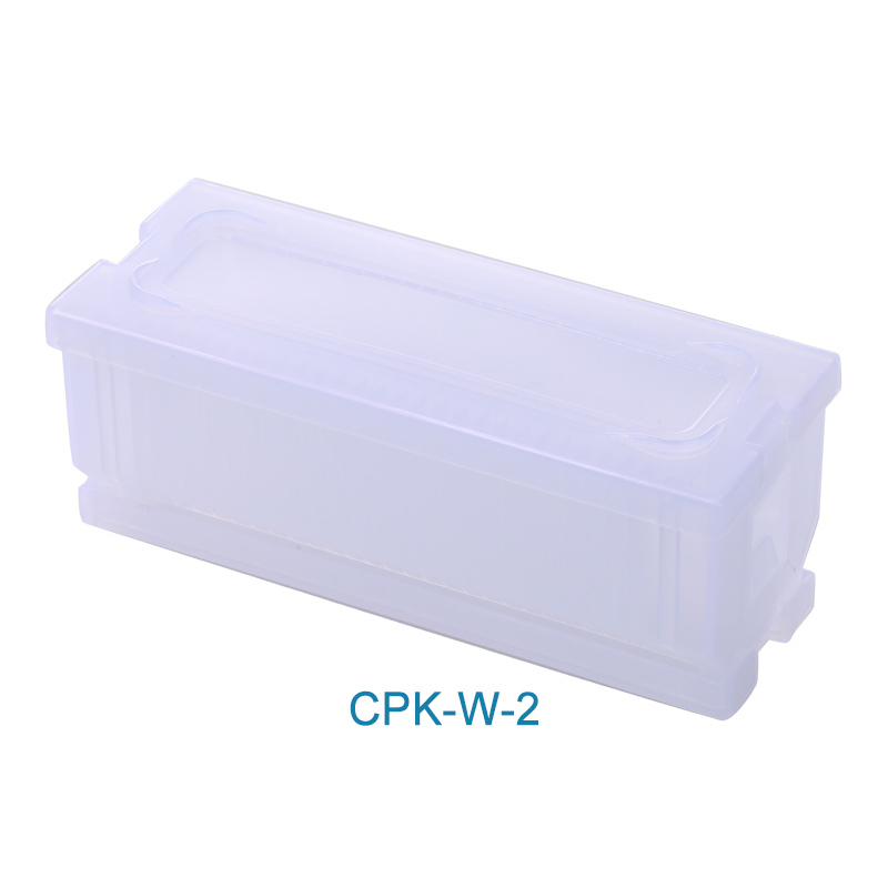 2-Inch Wafer Carrier (25 Wafers)
Semiconductor Manufacturing Equipment
Cryspack
The 2-inch wafer carrier for 25 wafers packages, stores, transfers or displays precision devices and stores, transfers and transports wafers and circular thin sheets. See this page's specifications for dimensions, materials and structure. Contact Kangpaike to confirm samples, specifications, materials or customization.
-
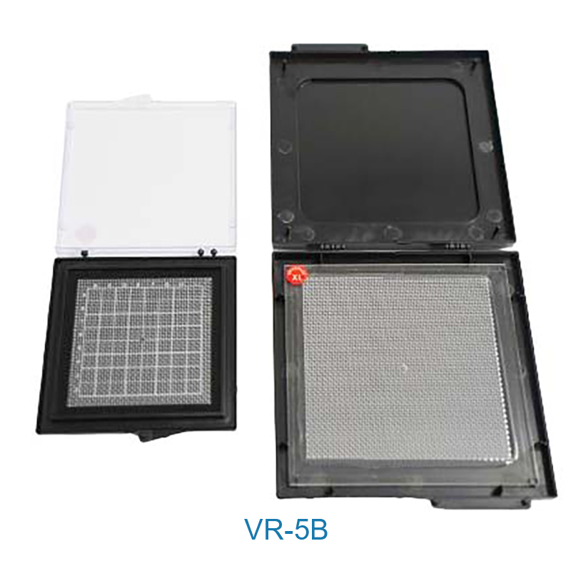 5-Inch Wafer and Large-Substrate Acrylic Vacuum-Release Plate
Semiconductor Manufacturing Equipment
Cryspack
The acrylic vacuum-release plate for 5-inch wafers and large substrates packages, stores, transfers or displays precision devices and holds and releases wafers and large substrates. See this page's specifications for dimensions, materials and structure. Contact Kangpaike to confirm samples, specifications, materials or customization.
-
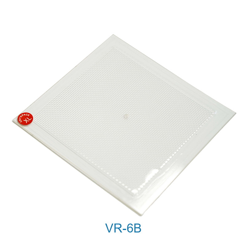 Wafer and Large-Substrate Acrylic Vacuum-Release Plate (6×6 Inches)
Semiconductor Manufacturing Equipment
Cryspack
The 6×6-inch acrylic vacuum-release plate for wafers and large substrates packages, stores, transfers or displays precision devices and holds and releases wafers and large substrates. See this page's specifications for dimensions, materials and structure. Contact Kangpaike to confirm samples, specifications, materials or customization.
-
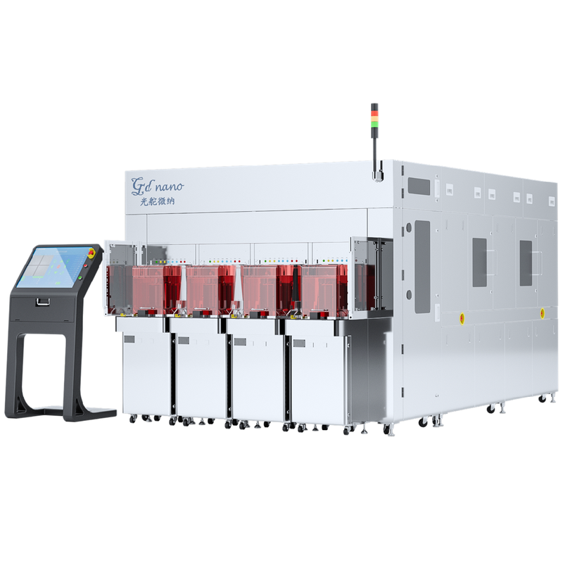 Fully Automatic Nanoimprint Equipment
Semiconductor Manufacturing Equipment
Gdnano
Equipment Alignment and Imprinting Capability: ≤2um
1. 8/12 compatibility: Easily exchange 8inch and 12inch substrates. 2. Modular design: Integrates EFEM, spin coater, HP, CP, NIL, Frame loading Unit, Pre-aligner and RF-reader. Additional submodules expand production capacity. 3. Precision: Minimum imprint linewidth 30nm; aspect ratio 10:1; dimensional deviation from master <3%; alignment accuracy ±2um. 4. Production: UPH 30 with excellent stability. 5. Fully automatic: Guangduo's in-house intelligent software automates all actions and provides real-time monitoring of key processes. 6. Cleanliness: Chamber environment reaches class 1; data deviation from master <3%; interwafer dimensional deviation <3%. Alignment/imprinting capability ≤2um. A precision stage provides stable alignment and eccentricity compensation.
Related Articles
Founded in November 2017, TIANJIN H‑CHIP TECHNOLOGY GROUP CORPORATION is a professional manufacturing‑service provider dedicated to micro‑nano optoelectronic chips. It holds multiple prestigious qualifications, including National High‑Tech Enterprise, one of Tianjin’s first Gazelle‑certified Enterprises, Specialized‑Refined‑Differentiated‑Innovative SME, and Leading Enterprise for Strategic Emerging Industries.
GYOPTICS 30 W collimated isolator is a highly‑reliable passive optical component optimized for 1064 nm high‑power laser systems. Characterized by low insertion loss and superior backward‑light suppression capability, it effectively blocks reflected light traveling back toward the laser resonator, eliminating back‑reflection‑induced instability and protecting fiber or solid‑state laser sources during long‑term operation.
Fomoptic delivers integrated one‑stop optical solutions covering precision optical fabrication and custom vacuum coating services. Supported by complete processing production lines, comprehensive metrology equipment and experienced engineering team, we provide full‑chain customized components, ranging from blank shaping, ultra‑precision polishing to thin‑film coating, for laser systems, infrared imaging, industrial optics and scientific‑research projects.
Founded in 2003, BWT Beijing Optoelectronics adheres to the mission "Let Dreams Fly With Light" and vision of becoming a Global Leader in Laser Solutions, guided by the core value "Innovate to Achieve Extraordinary".
Loading...
Name
Phone
Organization
Use Case

Database Platform