
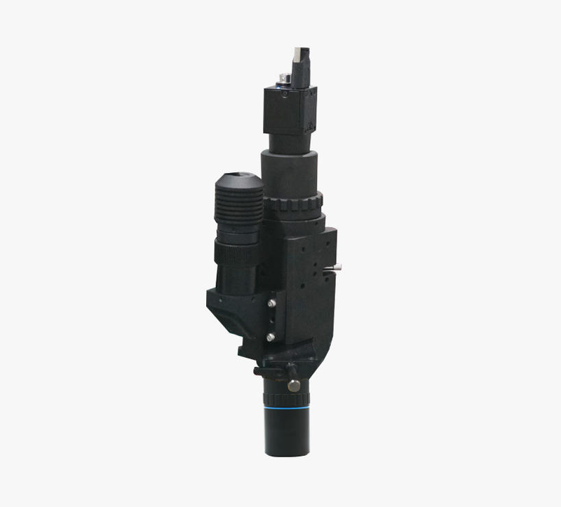
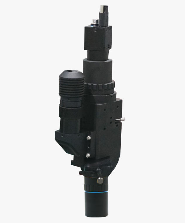
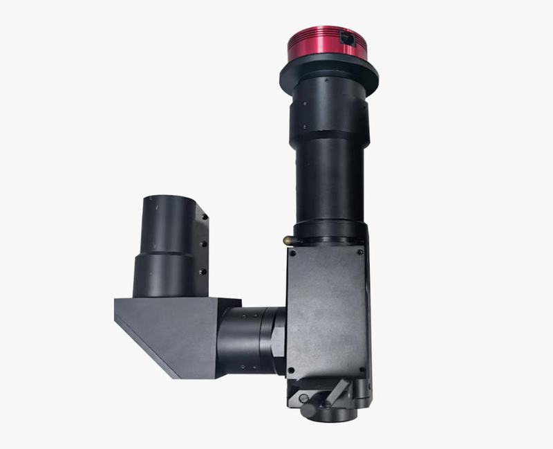
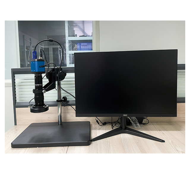
Differential interference contrast (DIC) microscope
The working principle of a DIC differential interference contrast microscope is to use the coherent light interference phenomenon to convert changes in sample surface topography into optical path differences. A position-sensitive detector is used to detect changes in the intensity of the light wavefront, and digital signal processing is used to obtain changes in the height of the sample surface.
 Save to Favorites
Overview
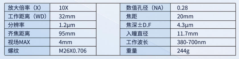
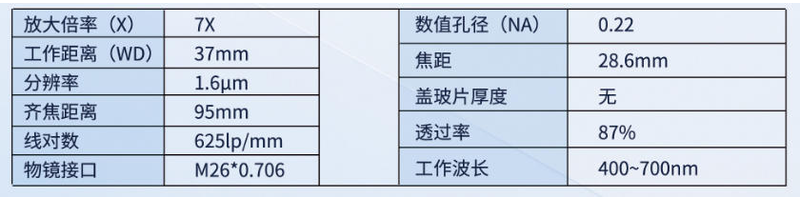
Specifications
| Parameter | Value |
|---|---|
| Magnification (X) [10X] | 10X |
| Working distance (WD) [10X] | 32 mm |
| Resolution [10X] | 1.2 μm |
| Parfocal distance [10X/7X] | 95 mm |
| Field of view MAX [10X] | 4 mm |
| Thread [10X] | M26X0.706 |
| Numerical aperture (NA) [10X] | 0.28 |
| Focal Length [10X] | 20 mm |
| Depth of focus ±D.F [10X] | 4.3 μm |
| Entrance pupil diameter [10X] | 11.7 mm |
| Operating Wavelength [10X] | 380-700nm |
| Weight [10X] | 244 g |
| Magnification (X) [7X] | 7X |
| Working distance (WD) [7X] | 37 mm |
| Resolution [7X] | 1.6 μm |
| Line pairs [7X] | 625 lp/mm |
| Objective lens interface [7X] | M26*0.706 |
| Numerical Aperture (NA) [7X] | 0.22 |
| Focal Length [7X] | 28.6 mm |
| Cover Glass Thickness [7X] | None |
| Transmittance [7X] | 87 % |
| Operating Wavelength [7X] | 400~700 nm |
Applications
Key Features
Datasheet
Please provide your email to download the datasheet.
Invalid email format. Please try again.
Supplier Information
Related Products
-
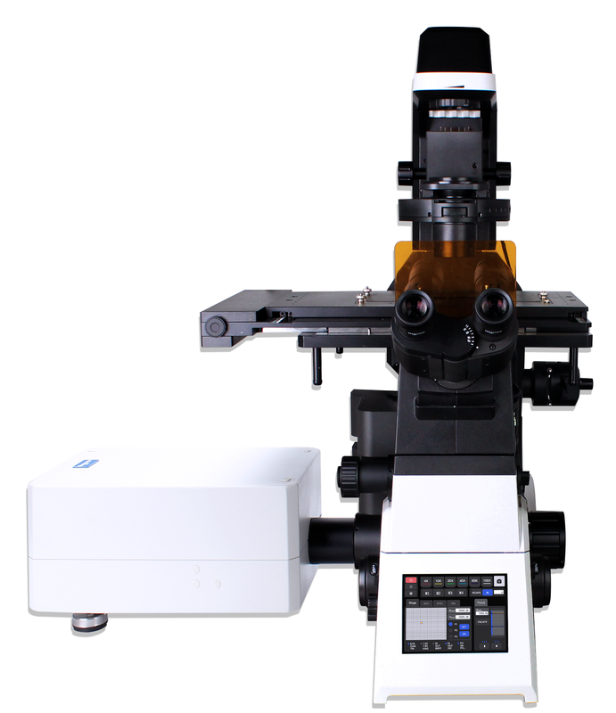 NCF1000 Laser Confocal Microscope
Microscopes
Yxopt
The demand for analysis of tissues, organs, and model organisms in life science research is growing, and efficient imaging has become key to scientific breakthroughs. Large-sample imaging needs to balance a broader range and faster speed to precisely capture dynamic intracellular reactions. To this end, we launch the NCF1000 series laser confocal microscope to meet the high-throughput, high-quality imaging needs of modern biology. Large field of view, high resolution, and fast speed bring better images, clearer contrast, and more realistic colors, helping you explore the cellular nanoscale in depth, intuitively and accurately analyze life processes, and expand the boundaries of scientific research.
-
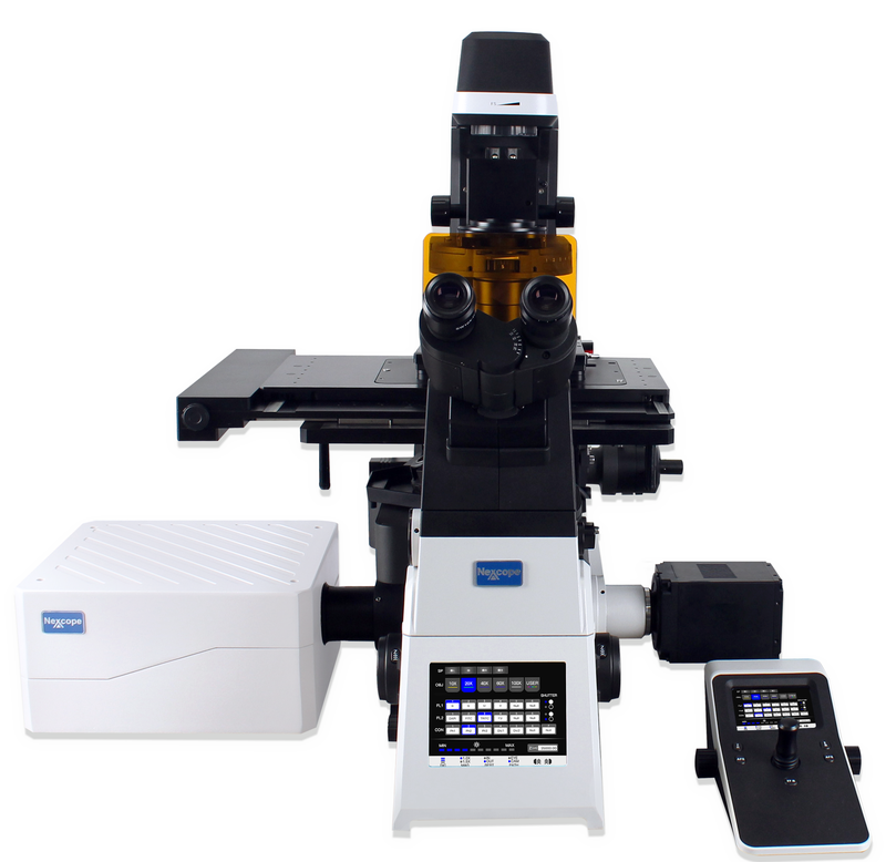 NCF2000 Laser Confocal Microscope
Microscopes
Yxopt
As life science research advances to deeper levels and broader scopes, efficient imaging technology has become a core element of scientific breakthroughs. Acquiring large-sample images requires both expanding the imaging range and greatly shortening acquisition time, so as to precisely capture the dynamic reactions inside cells. The NCF2000 laser confocal microscope is a comprehensive innovation over the NCF1000, built to meet the ultra-high demands of high-throughput, high-quality imaging in modern biological research. Imaging speed and phototoxicity optimization: it adopts resonance scanning technology, greatly shortening image acquisition time and achieving extremely high imaging efficiency. At the same time, it significantly reduces phototoxicity, making it friendlier to live cell samples and enabling long-term dynamic observation. Resolution and signal-to-noise ratio improvement: the newly upgraded spatial array confocal scanning head features low-noise, high-sensitivity spatial detection capability. It effectively improves the image signal-to-noise ratio and resolution, allowing you to easily capture subtle structures and key details in samples. Whether it is the panoramic presentation of large-area ultrastructure or the precise recording of rapidly changing life processes, the NCF2000 can provide professional, clear confocal imaging solutions, helping you explore the unknown fields of life science and reveal more secrets of life.
-
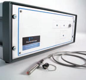 RamanMicro 200 Raman Microscope (PerkinElmer)
Microscopes
Gzbiaoqi
Optical system: The world's only two-dimensional dispersive Raman spectrometer combining an echelle grating and a two-dimensional array CCD detector, integrating the features of wide band, high resolution and fast detection speed. It abandons the conventional method of acquiring high-resolution spectra by measuring different spectral bands multiple times and then stitching them together, and can acquire a high-resolution Raman spectrum covering the entire band within one second. Dispersion system: Adopts echelle grating technology with no moving elements, ensuring high system stability. Detector: High-sensitivity two-dimensional CCD detector, enabling simultaneous acquisition of data across the entire spectral range, avoiding spectral distortion
-
 Electron Microscope
Microscopes
Cnzhongxing
Related Articles
Medical disposable‑device manufacturers have long demanded high‑performance interconnect accessories for single‑use equipment. The newly‑launched REDEL‑P disposable‑connector family addresses this requirement and delivers premium‑grade electrical connections for varied one‑time‑use medical instruments.
On November 28, 2024, the 3rd China Laser Star Enterprise Summit & Advanced Laser Processing Technology Summit, an annual influential event in the laser industry, was grandly held in Wuhan Optics Valley.
Driven by the rapid upgrading of intelligent vehicles, optoelectronic sensing technologies represented by laser sensing and infrared thermal imaging have become core pillars for high-level autonomous driving and smart cockpit iteration. Leveraging automotive-grade optoelectronic R&D advantages, Pilot Technology Group launches the VITAL intelligent vehicle solution. By integrating high-power VCSEL laser chips and vehicle infrared night-vision thermal imagers, the system comprehensively enhances vehicle environmental perception and realizes safer, smarter and more comfortable driving experiences.
Fluoride crystal glass and K9 optical glass are two core optical substrates widely used in precision optical systems, laser equipment and photoelectric scientific research.
Loading...
Name
Phone
Organization
Use Case

Database Platform