
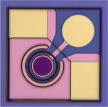
25Gbps InGaAs PIN Photodiode Chip
The 25Gbps InGaAs PD photodiode chip uses a front-illuminated mesa structure with
 Save to Favorites
Overview
Specifications
| Parameter | Value |
|---|---|
| Reverse Breakdown Voltage - Test Condition: Id=10uA,no illumination | Min 10V |
| Dark Current - Test Condition: Vr=-5 | Typ 1nA; Max 5nA |
| Responsivity - Test Condition: 1550nm, 1uW, M=1 | Min 0.7A/W; Typ 0.75A/W |
| -3 dB Bandwidth - Test Condition: Vr=-5 | Min 18GHz |
| Capacitance - Test Condition: Vr=-5V, f=1MHz | Max 0.1pF |
Applications
Key Features
Datasheet
Please provide your email to download the datasheet.
Invalid email format. Please try again.
Supplier Information
Related Products
-
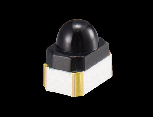 3020PD-608
Photodiodes
Xs-ir
Forward Voltage (VF) [Ta = 25 ℃]: 1.5 V Reverse voltage (VR) [Ta = 25 ℃]: 35 V Operating temperature (TOPR): -40 °C ~ 100 °C
-
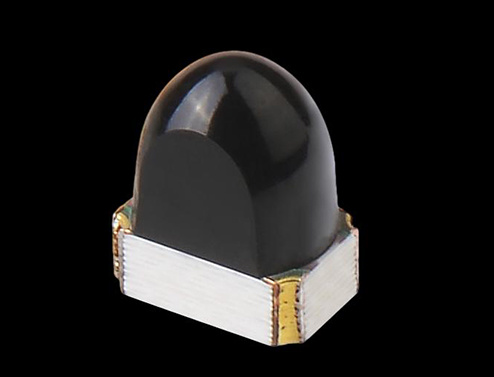 3020pd-806
Photodiodes
Xs-ir
Forward voltage (VF) [Absolute maximum ratings; Ta = 25 ℃]: 1.5 V Reverse voltage (VR) [Absolute maximum ratings; Ta = 25 ℃]: 35 V Operating temperature (TOPR) [Absolute Maximum Ratings]: -40 ℃ to 100 ℃
-
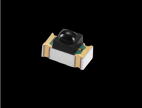 XS-PD02D16-600
Photodiodes
Xs-ir
Power Dissipation (Pd) [Ta = 25 ℃]: 150 mW Reverse voltage (VR) [Ta = 25 ℃]: 35 V Operating Temperature (TOPR): -40 ~ 100 ℃
Related Articles
Medical disposable‑device manufacturers have long demanded high‑performance interconnect accessories for single‑use equipment. The newly‑launched REDEL‑P disposable‑connector family addresses this requirement and delivers premium‑grade electrical connections for varied one‑time‑use medical instruments.
On November 28, 2024, the 3rd China Laser Star Enterprise Summit & Advanced Laser Processing Technology Summit, an annual influential event in the laser industry, was grandly held in Wuhan Optics Valley.
Driven by the rapid upgrading of intelligent vehicles, optoelectronic sensing technologies represented by laser sensing and infrared thermal imaging have become core pillars for high-level autonomous driving and smart cockpit iteration. Leveraging automotive-grade optoelectronic R&D advantages, Pilot Technology Group launches the VITAL intelligent vehicle solution. By integrating high-power VCSEL laser chips and vehicle infrared night-vision thermal imagers, the system comprehensively enhances vehicle environmental perception and realizes safer, smarter and more comfortable driving experiences.
Fluoride crystal glass and K9 optical glass are two core optical substrates widely used in precision optical systems, laser equipment and photoelectric scientific research.
Loading...
Name
Phone
Organization
Use Case

Database Platform