


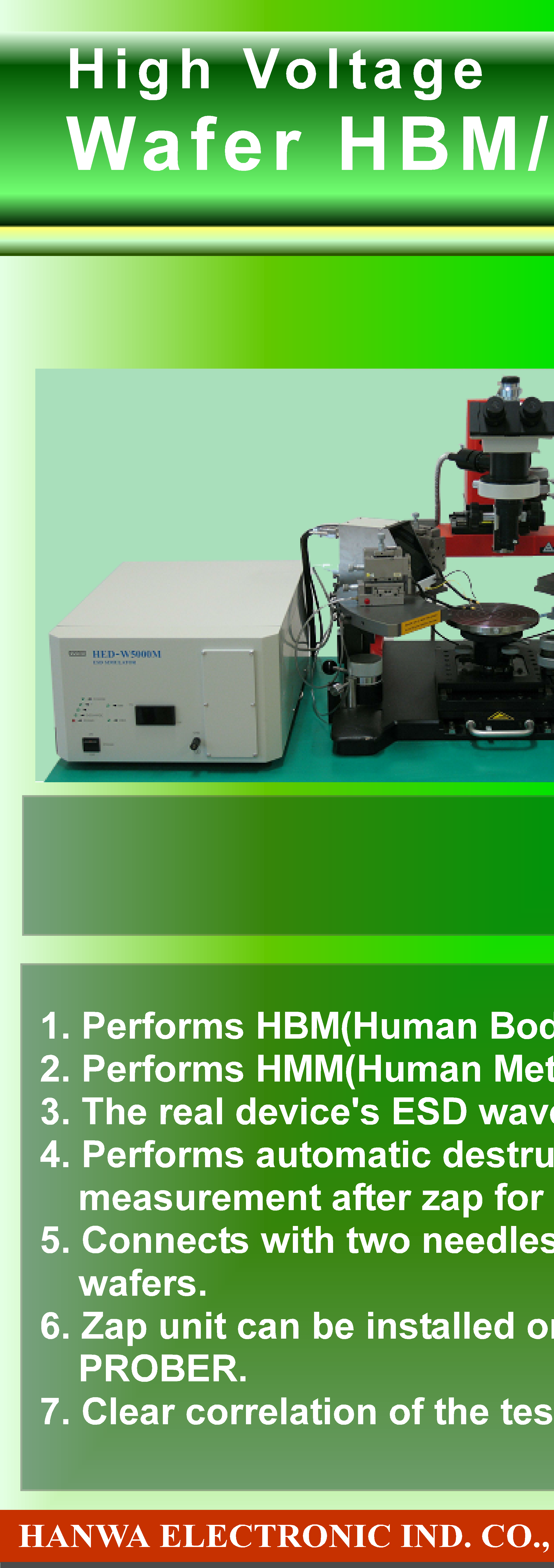
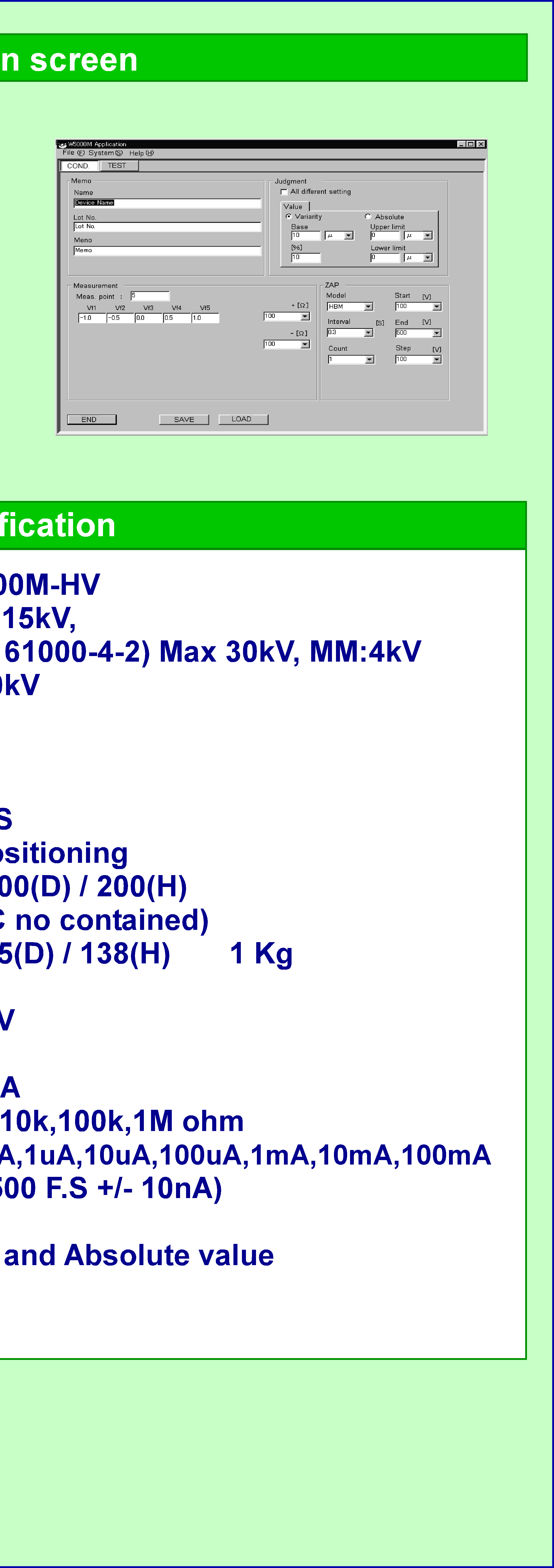
HED-W5000M-HV
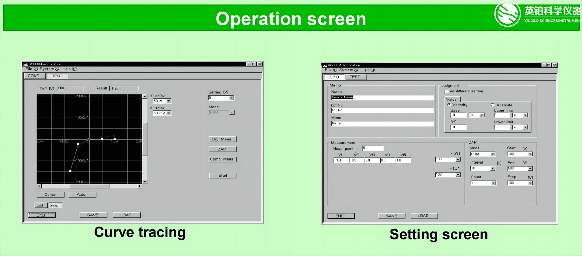
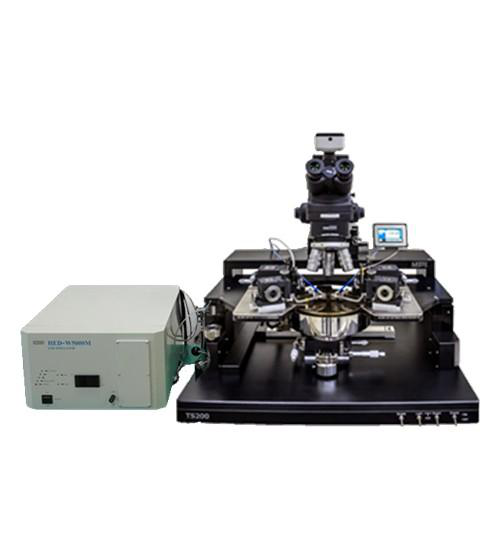
The HED-W5000M-HV is a high-voltage wafer HBM/HMM tester designed for precise ESD testing of packages and wafers. It supports HBM and HMM testing with advanced features for destructive evaluation and waveform display.
 Save to Favorites
Overview
Specifications
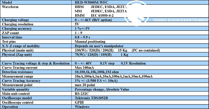
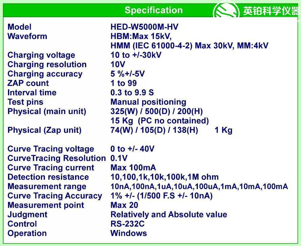
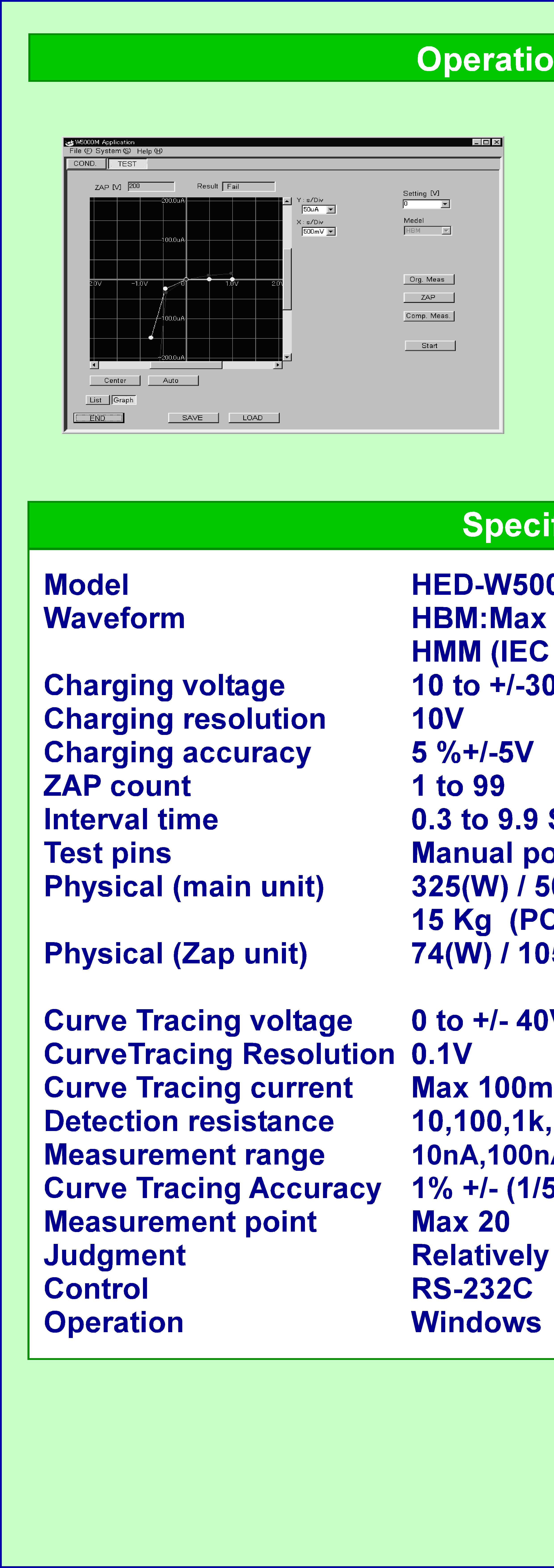
| Parameter | Value |
|---|---|
| Model | HED-W5000M-HV |
| Waveform | HBM: Max 15kV, HMM (IEC 61000-4-2): Max 30kV, MM: 4kV |
| Charging Voltage | 10 to +/-30kV |
| Charging Resolution | 10V |
| Charging Accuracy | 5% +/-5V |
| Zap Count | 1 to 99 |
| Interval Time | 0.3 to 9.9s |
| Test Pins | Manual positioning |
| Physical (Main Unit) | 325(W)/500(D)/200(H), 15Kg (PC not contained) |
| Physical (Zap Unit) | 74(W)/105(D)/138(H), 1Kg |
| Curve Tracing Voltage & Step Resolution | 0 to +/-40V, 0.1V step, 0.1V resolution |
| Curve Tracing Current | Max 100mA |
| Detection Resistance | 10,100,1k,10k,100k,1M ohm |
| Measurement Range | 10nA,100nA,1uA,10uA,100uA,1mA,10mA,100mA |
| Curve Tracing Accuracy | 1% +/- (1/500 F.S +/-10nA) |
| Measurement Point | Max 20 points |
| Judgment | Relatively and Absolute Value |
| Control | RS-232C |
| Operation | Windows |
Applications
Key Features
Datasheet
Supplier Information
Related Products
-
 Electro-Optic Q-Switch Pockels Cell Module
Other
Yokogawa
Electro-Optic Q-Switch Pockels Cell Module
Other
Yokogawa
Crystal Material: KD*P/BBO Operating Wavelength Range: 300-1100nm Clear Aperture: 8mm×8mm
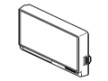
The Electro-Optic Q-Switch Pockels Cell Module is a fast optical switching device based on the linear electro-optic (Pockels) effect in a nonlinear crystal. As shown in the drawing, the device is packaged in a compact rectangular metal housing with a large, clear optical aperture and a side-mounted high-voltage electrical connector, allowing convenient integration into a laser cavity. When a high-voltage pulse is applied, the crystal induces a controlled phase retardation of the transmitted polarized beam; in combination with intracavity polarizers, the module acts as an ultrafast intracavity loss switch. It is widely used for Q-switching of solid-state lasers, cavity dumping, pulse picking and regenerative amplifier injection/ejection. Key characteristics include low half-wave voltage, high extinction ratio, high optical transmission, nanosecond-level switching speed and high laser damage threshold, making it suitable for industrial, medical, scientific and LiDAR laser systems. Note: the source material contains only a product outline drawing without a written datasheet; the specifications listed are typical values for this product class and should be confirmed against the manufacturer's official datasheet.
-
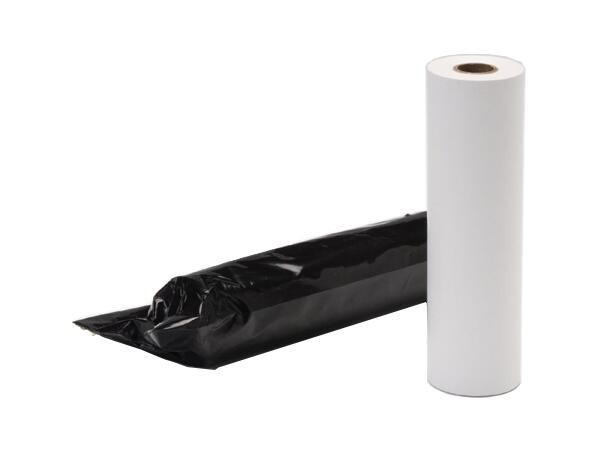 Laser Photoplotter Photosensitive Film Roll
Other
Yokogawa
Laser Photoplotter Photosensitive Film Roll
Other
Yokogawa
Product Form: Roll Packaging Method: Black light-tight sealed bag Core Type: Cardboard core
The product shown is a roll of light-sensitive (photosensitive) recording film, supplied together with a black light-tight protective bag. The film is wound on a standard cardboard core in roll form, with a smooth, uniformly coated white/ivory surface. Because the emulsion is sensitive to light, the roll is packaged in an opaque black sealed bag to prevent exposure during storage and transportation. This type of film is designed for high-resolution laser imaging equipment such as laser photoplotters, imagesetters and phototypesetters, where a laser beam scans the film surface to record fine circuit patterns, text or graphics. After laser exposure, the film is developed to produce high-contrast, high-density images used as phototools or film positives in PCB fabrication and printing plate making.
-
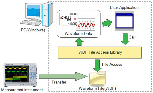 WDF File Access Library
Other
Yokogawa
WDF File Access Library
Other
Yokogawa
Product Type: API software library (Dynamic Link Library, DLL) Supported File Format: WDF (waveform data file saved on Yokogawa measurement instruments) Supported Operating System: Windows 10 (32 bit or 64 bit) / Windows 11, English or Japanese version
The WDF File Access Library is a free API (Application Program Interface) provided as a DLL (Dynamic Link Library) that enables user applications on a Windows PC to acquire data from waveform data files (WDF) saved on Yokogawa measurement instruments. By linking the DLL, developers can build application software with functions such as getting measuring conditions and getting waveform data from recorded WDF files accessible over the PC storage environment. Dedicated DLLs are provided for waveform data saved with the DL850E series, DL350, DL950, SL2000, Yokogawa's Xviewer software, and the DLM3000, DLM3000HD, DLM5000 and DLM5000HD series. The library offers functions for getting measuring date/time, measuring trace (channel) information, measuring points, time data/measuring data, units of the time axis/measuring axis, and resolutions of the time axis/measuring axis. The software package includes the library body (DLL), DLL import library (.lib), the prototype declaration header file (WDFAPIPublic.h), and sample code for explicit DLL linking (WDFAPIWrapper.cpp).
-
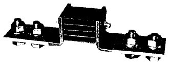 Optical Rail System with Adjustable Optical Mounts
Other
Yokogawa
Optical Rail System with Adjustable Optical Mounts
Other
Yokogawa
Number of Adjustable Optical Mounts: 4 Number of Central Optical Units: 1 Rail Layout: Linear, dual-section (left/right of central unit)
Based on the provided image, the product is a linear optical rail (optical bench) system consisting of a long rail base, four adjustable optical mounts with vertical posts arranged on both sides of the rail, and a central enclosed optical unit with a multi-slot housing. The rail structure allows optical components such as lenses, mirrors or filters to be positioned precisely along a common optical axis. Note: the source image is severely degraded (high-threshold silhouette) and no text, brand or detailed specifications are legible; the extraction is therefore based on the visible mechanical structure of the product.
-
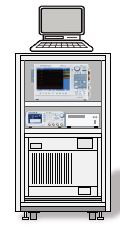 Rack-Mounted Optoelectronic Test and Measurement System
Other
Yokogawa
Rack-Mounted Optoelectronic Test and Measurement System
Other
Yokogawa
System Architecture: Floor-standing standardized instrument rack with integrated multi-layer modules Control Computer: Top-mounted desktop workstation with monitor and keyboard Upper Measurement Module: Analysis/measurement instrument with integrated display and front-panel controls
The product shown is a floor-standing, rack-mounted optoelectronic test and measurement platform. The system integrates multiple instruments into a single standardized cabinet: an upper measurement/analysis module with an integrated display, a middle layer containing benchtop instruments (a display/readout unit and a source or control unit), and a high-power lower module with a front-panel ventilation grille, which indicates forced-air cooling for driving or testing high-power devices. A dedicated computer workstation (monitor and keyboard) is mounted on top of the cabinet for system control, data acquisition and analysis. The whole rack is supported by leveling feet for stable laboratory or production-floor installation. Please note: the provided image contains no legible brand name, model number or numerical technical data; the description and parameters below are therefore based on the visible system configuration, and detailed electrical/optical specifications should be confirmed with the manufacturer's official datasheet.
Related Articles
Shanghai Connet Laser Technology Co., Ltd. focuses on technological innovation, delivering cutting-edge photonic products & solutions for industrial lasers, LiDAR, fiber optic sensing, coherent telecom, cold atom physics and precision spectroscopy research & mass manufacturing.
A solid-state laser is one of the most common and reliable laser types used in modern industry, medical equipment, and scientific research. Unlike gas or fiber lasers, it uses solid materials as its gain medium to generate stable, high-brightness laser beams. Thanks to its high precision, long lifespan, and compact structure, solid-state lasers have become a mainstream solution for high-precision laser processing and optical systems.
Looking for a market-verified 808nm pump laser diode? This guide introduces HAUCORE DM-8E5A-8OD (HGLD-808-COS-D-5W), its core advantages, key specs and mainstream industrial, medical & research applications.
Founded in 2003, BWT Beijing Optoelectronics adheres to the mission "Let Dreams Fly With Light" and vision of becoming a Global Leader in Laser Solutions, guided by the core value "Innovate to Achieve Extraordinary".
Loading...
Name
Phone
Organization
Use Case

Database Platform