
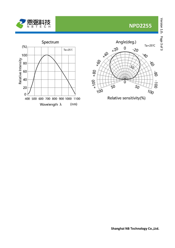
NPD2255 Dual-Area PD
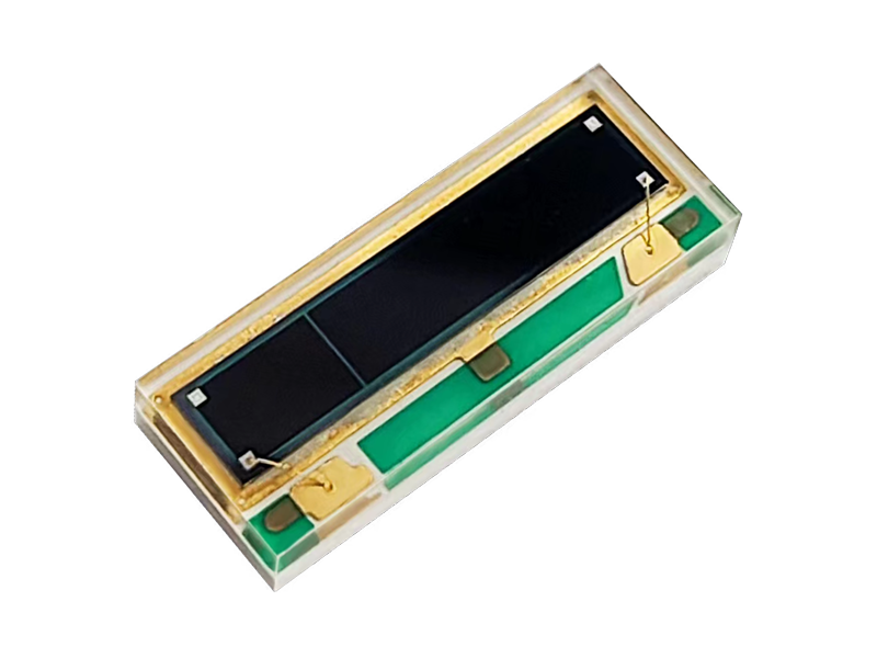
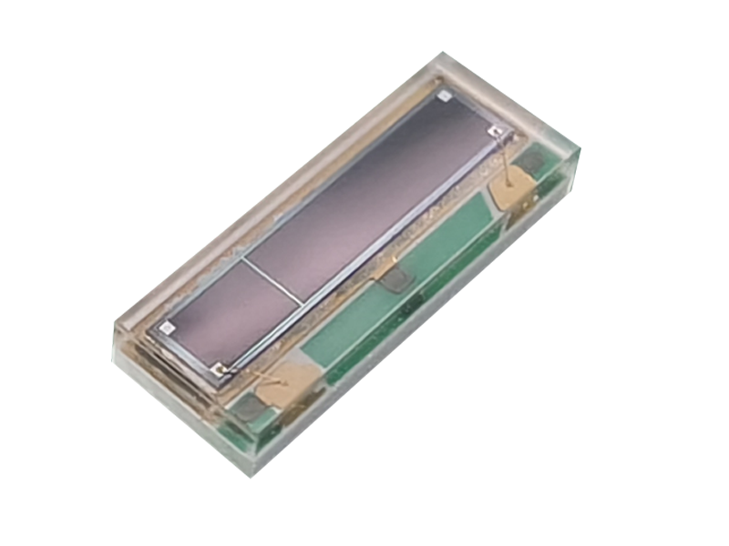
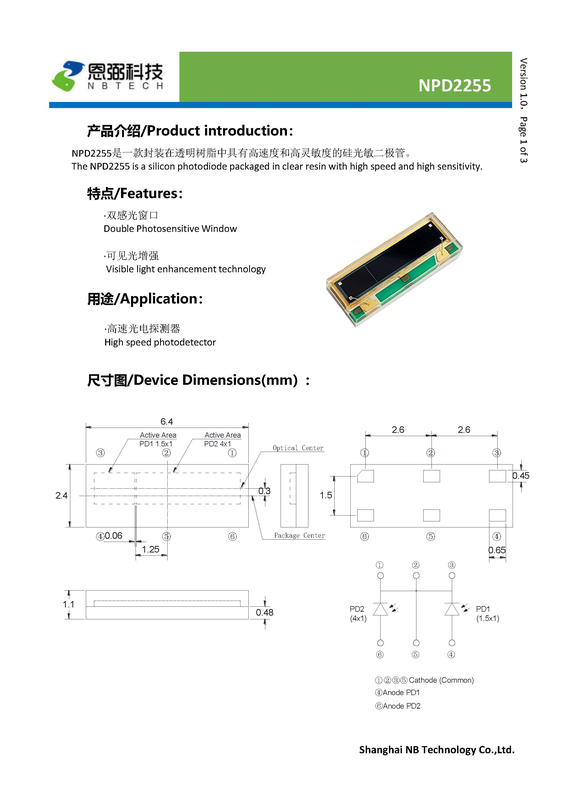
NPD2255 is a receiver custom-developed for background-suppression (BGS) sensors. It has two asymmetric photosensitive regions that effectively define responsive and nonresponsive areas, or working and suppression zones. Other asymmetric Dual PD options are available: NPD2235: 1.3×1.0 + 1.3×2.5; NPD2255: 1.0×1.5 + 1.0×4.0; NPD2233: 1.0×3.3, comprising two joined triangles. No dimensional unit is supplied in this description.
 Save to Favorites
Overview
Specifications
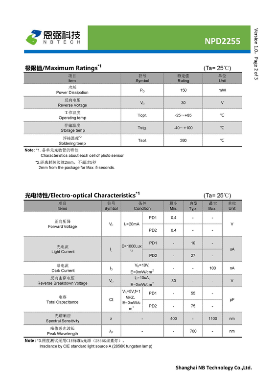
| Parameter | Value |
|---|---|
| Power Consumption P_D [Reference; Maximum Ratings; Ta=25°C; Photodetector Characteristics of Each Cell] | 150 mW |
| Reverse Voltage V_R [Reference; Maximum Ratings; Ta=25°C; Photodetector Characteristics of Each Cell] | 30 V |
| Operating Temperature Topr. [Reference; Maximum Ratings; Ta=25°C; Photodetector Characteristics of Each Cell] | -25~+85 °C |
| Storage Temperature Tstg. [Reference; Maximum Ratings; Ta=25°C; Photodetector Characteristics of Each Cell] | -40~+100 °C |
| Soldering Temperature Tsol. [Reference; Maximum Ratings; Ta=25°C; Photodetector Characteristics of Each Cell; 2mm from Package Edge, No More Than 5 Seconds] | 260 °C |
| Forward Voltage Drop V_F [Reference;Electro-optical Characteristics;Ta=25°C;Photosensitive Device per Cell;PD1;I_F=20mA] | min:0.4 V |
| Photocurrent I_L [Reference;Electro-optical Characteristics;Ta=25°C;Characteristics of Each Photosensitive Cell;PD1;E=1000Lux;CIE Standard Illuminant A,Chinese2856K Halogen Lamp/English2856K Tungsten Lamp] | typical:10 μA |
| Capacitance Ct [Reference;Electro-optical Characteristics;Ta=25°C;Characteristics of Each Photosensitive Cell;PD1;V_R=5V;f=1MHZ;E=0mW/cm²] | typical:55 pF |
| Forward Voltage Drop V_F [Reference;Electro-optical Characteristics;Ta=25°C;Photosensitive Device per Cell;PD2;I_F=20mA] | min:0.4 V |
| Photocurrent I_L [Reference;Electro-optical Characteristics;Ta=25°C;Characteristics of Each Photosensitive Cell;PD2;E=1000Lux;CIE Standard Illuminant A,Chinese2856K Halogen Lamp/English2856K Tungsten Lamp] | typical:27 μA |
| Capacitance Ct [Reference;Electro-optical Characteristics;Ta=25°C;Characteristics of Each Photosensitive Cell;PD2;V_R=5V;f=1MHZ;E=0mW/cm²] | typical:75 pF |
| Dark Current I_D [Reference; Electro-Optical Characteristics; Ta=25°C; Photodetector Characteristics of Each Cell; V_R=10V; E=0mW/cm²] | max:100 nA |
| Reverse Breakdown Voltage V_R [Reference; Electro-Optical Characteristics; Ta=25°C; Photodetector Characteristics of Each Cell; I_R=10μA; E=0mW/cm²] | min:30 V |
| Spectral Response λ [Reference; Electro-Optical Characteristics; Ta=25°C; Photodetector Characteristics of Each Cell] | min:400 nm; max:1100 nm |
| Peak Sensing Wavelength λ_P [Reference; Electro-Optical Characteristics; Ta=25°C; Photodetector Characteristics of Each Cell] | typical:700 nm |
Applications
Key Features
Datasheet
Supplier Information
Related Products
Related Articles
VCSEL, short for Vertical Cavity Surface Emitting Laser, is a widely used semiconductor laser component in modern optoelectronics. Unlike traditional edge-emitting lasers, VCSEL emits laser light vertically from its chip surface. Thanks to its low power consumption, stable beam quality, low cost, and easy integration, it has become the core light source for 3D sensing, wearable devices, and high-speed optical communication.
As fundamental refractive optical components, plano‑convex spherical lenses consist of one convex spherical surface and one flat surface.
FiDAR, the fiber‑optic radar vehicle positioning and tracking system developed by Jianhe Bafang, is a high‑sensitivity distributed fiber‑sensing solution designed for intelligent traffic road monitoring. It outputs real‑time spatial coordinates of every vehicle across the full road section around‑the‑clock, delivering a brand‑new sensing technology for vehicle‑road cooperation, smart highway construction and urban traffic management.
Raybowlaser, a professional manufacturer of high-power laser chips, has officially launched its upgraded new-generation 1470nm high-performance laser chip. Achieving groundbreaking progress in rated output power and wall-plug efficiency (WPE), this innovative laser chip delivers superior and reliable core light source solutions for medical cosmetology, industrial processing, agricultural applications and scientific research equipment.
Loading...
Name
Phone
Organization
Use Case

Database Platform