
NIR-V2303T Dual-Channel Photoelectric Switch
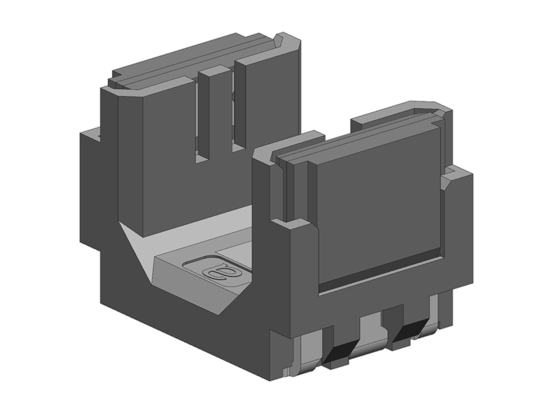
NIR-V2303T is a compact dual-channel transmissive optoelectronic switch integrating a high-output infrared LED and a high-sensitivity phototransistor. It enables noncontact detection of object presence/absence, movement direction and related parameters.
 Save to Favorites
Overview
Specifications
| Parameter | Value |
|---|---|
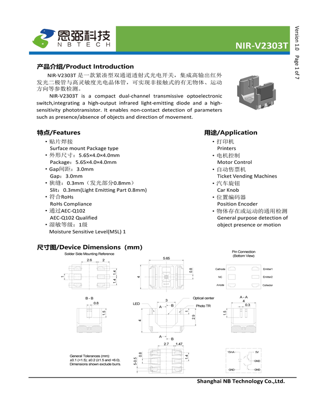
| Dimensions [Independent Features on Page 1; Not a Dimension Drawing] | 5.65 mm × 4.0 mm × 4.0 mm |
| Gap Spacing [Independent Features on Page 1] | 3.0 mm |
| Slit [Independent Features on Page 1; Emitting Section 0.8mm] | 0.3 mm |
| Moisture Sensitivity Level MSL | Grade 1 |
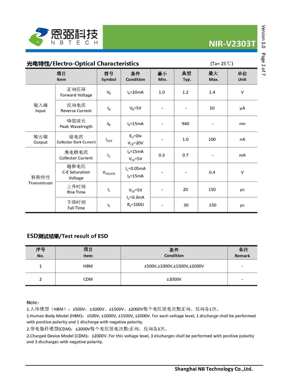
| Forward Voltage Drop V_F [Electro-Optical Characteristics; Ta=25°C; Input Side; I_F=20mA] | min:1.0 V; typical:1.2 V; max:1.4 V |
| Reverse Current I_R [Electro-Optical Characteristics; Ta=25°C; Input Side; V_R=5V] | max:10 μA |
| Peak Wavelength λ_P [Electro-Optical Characteristics; Ta=25°C; Input Side; I_F=15mA] | typical:940 nm |
| Dark Current I_CEO [Electro-Optical Characteristics; Ta=25°C; Output Side; E_V=0lx; V_CE=20V] | typical:1.0 nA; max:100 nA |
| Collector Current I_C [Electro-Optical Characteristics; Ta=25°C; Transfer Characteristics; I_F=15mA; V_CE=5V] | min:0.3 mA; typical:0.7 mA |
| Saturation Voltage V_CE(SAT) [Electro-Optical Characteristics; Ta=25°C; Transfer Characteristics; I_C=0.05mA; I_F=15mA] | max:0.4 V |
| Rise Time tr [Electro-Optical Characteristics; Ta=25°C; Conversion Characteristics; V_CE=5V; I_C=0.3mA; R_L=100Ω] | typical:20 μs; max:150 μs |
| Fall Time tf [Electro-Optical Characteristics; Ta=25°C; Conversion Characteristics; V_CE=5V; I_C=0.3mA; R_L=100Ω] | typical:30 μs; max:150 μs |
| HBM Test Conditions [One Forward/Reverse Discharge per Voltage; Table and Bilingual Notes All Give ±500V, ±1000V, ±1500V, ±2000V] | ±500V、±1000V、±1500V、±2000V |
| CDM Test Conditions [This Voltage Applied 3 Times in Each Forward and Reverse Direction] | ±2000V |
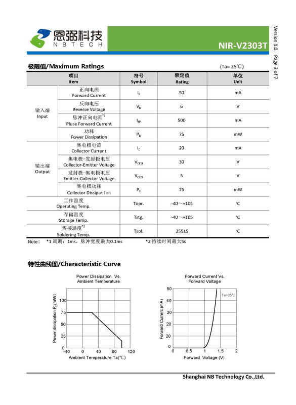
| Forward Current I_F [Maximum Ratings; Ta=25°C; Input End] | 50 mA |
| Reverse Voltage V_R [Maximum Ratings; Ta=25°C; Input End] | 6 V |
| Pulsed Forward Current I_FP [Maximum Ratings; Ta=25°C; Input Side; Period 1ms; Maximum Pulse Width 0.1ms] | 500 mA |
| Power Consumption P_D [Maximum Ratings; Ta=25°C; Input End] | 75 mW |
| Collector Current I_C [Maximum Ratings; Ta=25°C; Output End] | 20 mA |
| Collector-Emitter Voltage V_CEO [Maximum Ratings; Ta=25°C; Output End] | 30 V |
| Emitter-Collector Voltage V_ECO [Maximum Ratings; Ta=25°C; Output End] | 5 V |
| Collector Power Dissipation P_C [Maximum Ratings; Ta=25°C; Output End] | 75 mW |
| Operating Temperature Topr. [Maximum Ratings; Ta=25°C; Common] | -40~+105 °C |
| Storage Temperature Tstg. [Maximum Ratings; Ta=25°C; Common] | -40~+105 °C |
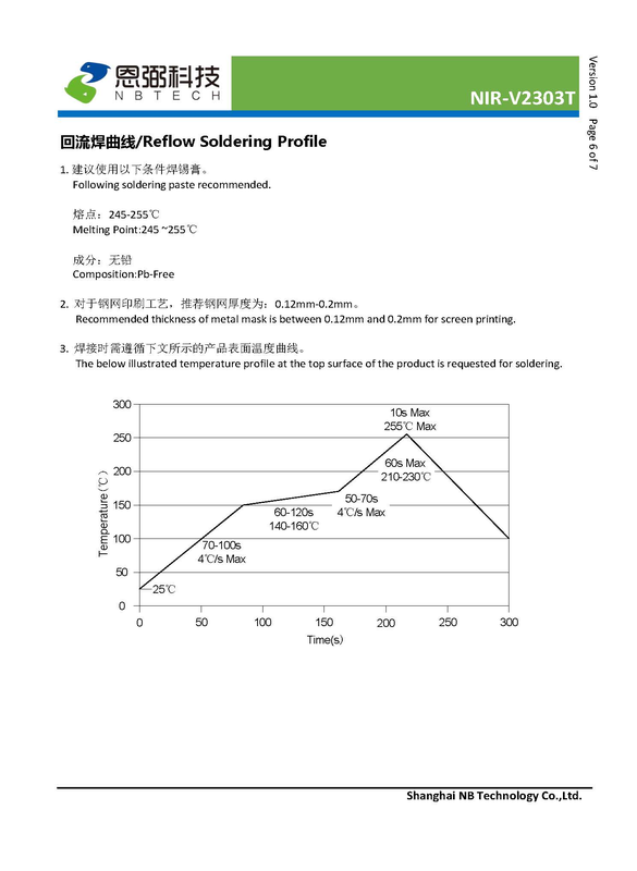
| Soldering Temperature Tsol. [Maximum Ratings; Ta=25°C; Common; Maximum Duration 5s] | 255±5 |
| Recommended Solder-Paste Melting Point [Independent Text Outside Curves on Page 6; Solder Paste Conditions, Not Product Temperature Ratings] | 245~255 °C |
| Recommended Solder-Paste Composition [Independent Text Outside Curves on Page 6] | Lead-Free / Pb-Free |
| Recommended Stencil Thickness [Stencil Printing Process; Independent Text Outside Curves on Page 6] | 0.12~0.2 mm |
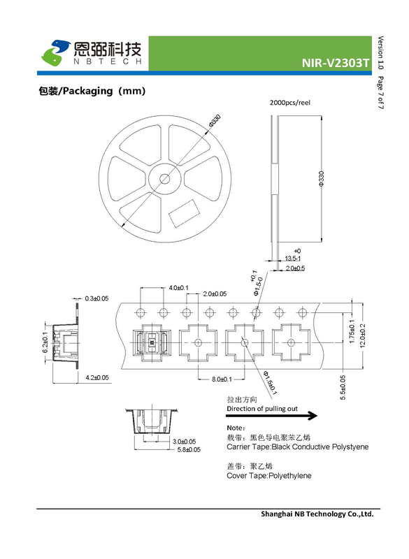
| Quantity per Package [Independent Text on Page 7] | 2000 pcs/reel |
| Carrier Tape [Note on Page 7] | Black Conductive Polystyrene (Source English: Black Conductive Polystyene) |
| Cover Tape [Note on Page 7] | Polyethylene |
Applications
Key Features
Datasheet
Supplier Information
Related Products
-
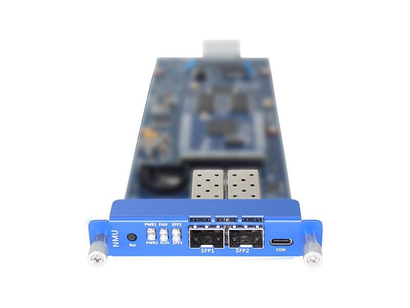 400G DCI BOX Main Control / Network Management Card FW8N
Optical Transport Equipment
Fiberwdm
Interface: Optical Ports: 2 SFP Ports; Serial Port: 1 Console Interface Network Management Method: NMS、Web、CL1、SNMP、 Environmental Requirements - Operating Temperature: -5℃~45℃
The FW8N network-management main control board connects to the management host, enabling real-time monitoring, configuration and management of all boards in a chassis. Its high-speed ARM processor provides strong data-processing capability. Management interfaces include the command-line interface labeled CU, a WEB browser interface and a graphical NMS. Server and standalone versions support networks of different sizes, providing suitable network-management solutions for operators and enterprise users.
-
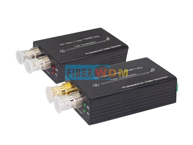 Mini 3G SDI Video-to-Optical Transceiver
Optical Transport Equipment
Fiberwdm
Power Supply - Power Consumption: 2W(max.) Power Supply - Power Supply Voltage: DC5-24V Input Light Center Wavelength: 1310nm
HD multimedia surveillance often requires long-distance uncompressed digital audio/video transmission. Ordinary cables suffer poor output, interference and limited reach. The 3G/HD-SDI-T/R optical pair carries 3G/HD-SDI over 1m–20km, addressing these problems. Low attenuation, broad bandwidth, interference resistance, security, compactness and light weight suit long distances/special environments while reducing construction cost and wiring complexity without sacrificing quality. 3G/HD-SDI-T is the transmitter and 3G/HD-SDI-R the receiver. The source also labels the transmitter 3G/HD-SDII-T. Together they send video over fiber without compression and faithfully reproduce the original signal.
-
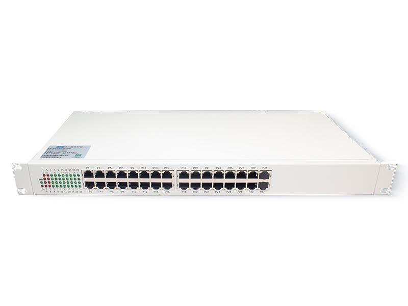 30-Channel Telephone + 4FE + 4E1 100-Megabit Network Telephone Optical Transceiver
Optical Transport Equipment
Fiberwdm
Product Function Description: Fiber Transmission of4 E1+30 Telephone Channels(Optional Magneto/Hotline Telephone,2/4-Wire Audio,Data,etc.)+4 Fast Ethernet Channels;1U Rack Equipment;RJ45 Telephone Interfaces(1 Channel per Port,Pin Assignment4/5) Service Port Description: 1 Optical Interface(155M,Optional Single/Dual-Fiber Transmission,FC or SC);4 E1 Interfaces(BNC);30 Telephone Interfaces(RJ45);4 Fast Ethernet Channels(Shared or Logically Isolated) Power Supply: AC-220V or DC48V Single Supply, Optional Dual AC220V/DC48V Supplies
The integrated service-access device provides 30 telephone channels, 4E1 and four 100M Ethernet channels. Proprietary large-scale integrated circuits use time-division multiplexing to encode Ethernet and E1 signals together for transmission over a fiber pair. Mixed services include 100M Ethernet, E1, voice, V35, data and two-/four-wire services, through optical or E1 transmission channels. A highly integrated 19-inch 1U chassis offers small size, low power, reliable operation and easy installation and use.
-
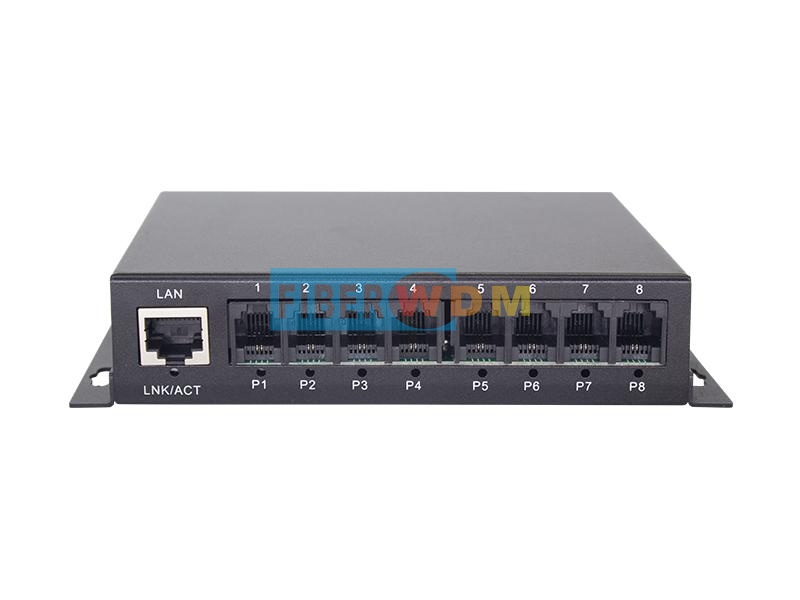 8-Channel Telephone-to-2-Channel Ethernet Optical Transceiver RD-08G2
Optical Transport Equipment
Fiberwdm
Ringing Voltage [FXS Subscriber Telephone Port / Orderwire Telephone Port]: 75 V Ringing Frequency [FXS Subscriber Telephone Port / Orderwire Telephone Port]: 25 Hz Two-Wire Input Impedance [FXS Subscriber Telephone Port / Orderwire Telephone Port]: 600Ω (Off-Hook)
This telephone-to-Ethernet optical terminal encapsulates voice in IP packets using UDP. The description states conversion of 1–8 voice services to two 100M Ethernet channels, labeled one RJ45 optical port and one 100M Ethernet optical connection, for communication within one subnet or across routed subnets. A separate port list gives eight RJ11 telephone ports, one 10/100/1000M adaptive Gigabit RJ45 Ethernet port and one FC/UPC optical port, single-mode, single-fiber bidirectional, 80KM. Power is external.
-
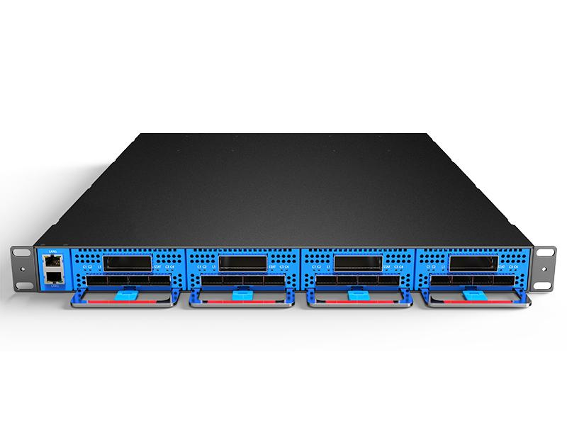 400G DCI BOX 1U Compact, Fully Configured 1.6T DCI BOX FW-8800
Optical Transport Equipment
Fiberwdm
Maximum Capacity per Chassis: Dual-Fiber Bidirectional 8X200G / 4X400G, 1.6Tbps Line-Side Modulation Mode: DP-QPSK@100G DP-16QAM@200G; DP-8QAM@200G; DP-QPSK@200G DP-16QAM@400G Line-Side Protocol: SD-FEC/OpenROADM/OpenZR+
FW-8800 is a compact 1U 400G DCI BOX, described as 1.6T fully populated, converting four 100G QSFP28 channels to 400G CFP2. Four 400G boards provide a stated bidirectional 3.2T service capacity. Dual-fiber point-to-point DWDM supports 48×400G at 100GHz or 64×400G at 75GHz. Independently developed by 广州市瑞东Email 科技有限公司 for 400G transmission, each board converts four 100G clients to one 400G line for multiservice, high-capacity networks. A 1U chassis holds four boards for up to 3.2Tbps service capacity. Uses include data-center DCI, metro access and aggregation, with intelligent optical-transport solutions across capacities/distances.
Related Articles
VCSEL, short for Vertical Cavity Surface Emitting Laser, is a widely used semiconductor laser component in modern optoelectronics. Unlike traditional edge-emitting lasers, VCSEL emits laser light vertically from its chip surface. Thanks to its low power consumption, stable beam quality, low cost, and easy integration, it has become the core light source for 3D sensing, wearable devices, and high-speed optical communication.
As fundamental refractive optical components, plano‑convex spherical lenses consist of one convex spherical surface and one flat surface.
FiDAR, the fiber‑optic radar vehicle positioning and tracking system developed by Jianhe Bafang, is a high‑sensitivity distributed fiber‑sensing solution designed for intelligent traffic road monitoring. It outputs real‑time spatial coordinates of every vehicle across the full road section around‑the‑clock, delivering a brand‑new sensing technology for vehicle‑road cooperation, smart highway construction and urban traffic management.
Raybowlaser, a professional manufacturer of high-power laser chips, has officially launched its upgraded new-generation 1470nm high-performance laser chip. Achieving groundbreaking progress in rated output power and wall-plug efficiency (WPE), this innovative laser chip delivers superior and reliable core light source solutions for medical cosmetology, industrial processing, agricultural applications and scientific research equipment.
Loading...
Name
Phone
Organization
Use Case

Database Platform