
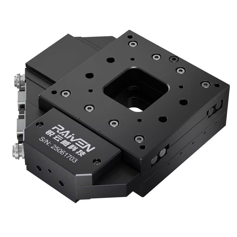
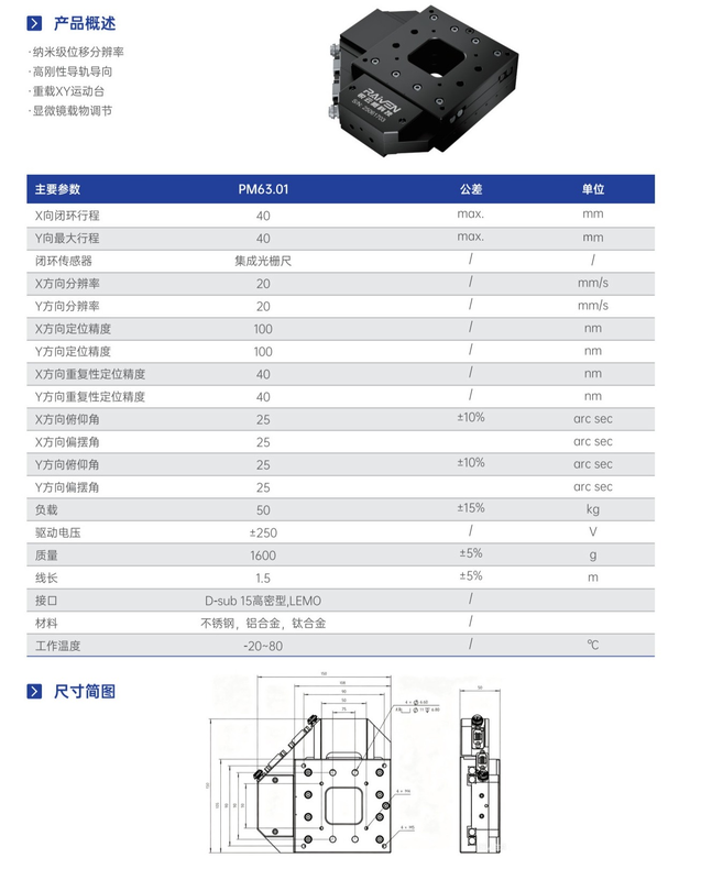
PM63.01-Series Two-Dimensional Specimen Stage
 Save to Favorites
Specifications
| Parameter | Value |
|---|---|
| X-Direction Closed-Loop Travel [max.] | 40 mm |
| Y-Direction Maximum Travel [max.] | 40 mm |
| Closed-Loop Sensor | Integrated Grating Scale |
| X-Direction Resolution | 20 mm/s |
| Y-Direction Resolution | 20 mm/s |
| X-Direction Positioning Accuracy | 100 nm |
| Y-Direction Positioning Accuracy | 100 nm |
| X-Direction Repeat Positioning Accuracy | 40 nm |
| Y-Direction Repeat Positioning Accuracy | 40 nm |
| X-Direction Pitch Angle [Tolerance ±10%] | 25 arc sec |
| X-Direction Yaw Angle [Tolerance ±10% (Originally Merged Vertically with Pitch Angle)] | 25 arc sec |
| Y-Direction Pitch Angle [Tolerance ±10%] | 25 arc sec |
| Y-Direction Yaw Angle [Tolerance ±10% (Originally Merged Vertically with Pitch Angle)] | 25 arc sec |
| Load [Tolerance ±15%] | 50 kg |
| Drive Voltage | ±250 V |
| Mass [Tolerance ±5%] | 1600 g |
| Cable Length [Tolerance ±5%] | 1.5 m |
| Interface | High-Density D-sub 15, LEMO |
| Material | Stainless Steel, Aluminum Alloy, Titanium Alloy |
| Operating Temperature | -20~80 °C |
Key Features
Datasheet
Please provide your email to download the datasheet.
Invalid email format. Please try again.
Supplier Information
Related Products
-
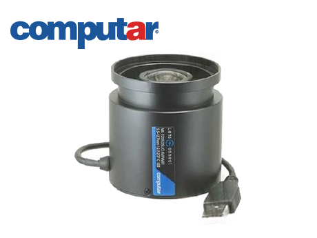 ML2Z0525UC-MPWIR
Motorized Stages
Daheng-imaging
Models Supporting the Autofocus Version: ML2Z0525R2C-MPWIR-IX0 Focusing Type: Motorized Zoom Resolution: 9M
Computar LensConnect Series 2/3-Inch 9000000-Pixel Motorized Lens
-
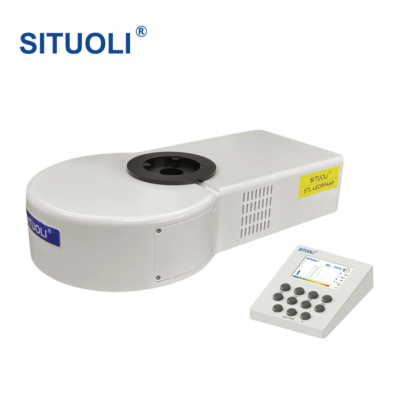 STL-LEDRFAA8 Upright 8-Position Motorized Fluorescence Module
Motorized Stages
Situoli
Light Source: Adjustable LED Service Life: >60000 小时 Light-Intensity Control Range: 0~99% Linear Adjustment
SITUOLI LED fluorescence illumination uses bright LEDs to reveal weak signals and offers observation comparable to advanced inverted fluorescence microscopes for varied dyes. Stable, efficient illumination and a short optical path improve brightness, excitation and detection; adjustable intensity reduces photobleaching. Unlike aging mercury lamps requiring calibration for comparisons over time, stable LEDs allow accurate comparisons. Life is60,000hours, stated as about20years at eight hours/day, versus about400 for mercury and2000 for metal halide, saving approximately90% or more in maintenance. Linear intensity adjustment and exact stored settings ensure repeatability. Intelligent temperature/humidity control monitors/displays values and automatically adjusts the internal environment for long-term stability. Live status simplifies operation; controlled intensity protects valuable samples. Actual hours are accurately displayed rather than overstated, with multiple data aiding research.
-
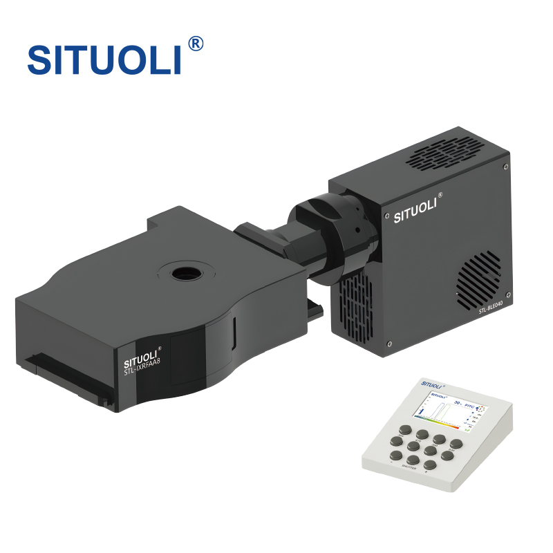 STL-IXRFAA8 Inverted 8-Position Motorized Fluorescence Module
Motorized Stages
Situoli
Light Source [Green Region Contains Parameters of the Optional STL-BLE040 Fluorescence Light Source]: Adjustable LED Service Life [Green Region Contains Parameters of the Optional STL-BLE040 Fluorescence Light Source]: >60000 小时 Light-Intensity Control Range [Green Region Contains Parameters of the Optional STL-BLE040 Fluorescence Light Source]: 0~99% Linear Adjustment
This LED fluorescence illumination unit uses integrated bright LEDs to reveal weak fluorescence. Switching excitation blocks by handle selects the matching LED. Freely adjustable linear intensity compensates for channel/dye efficiency; stored per-channel settings ensure repeatability. With multiband blocks, software selects source channels and brightness independently under equal exposure/gain for efficiency. Duty-cycle control reduces phototoxicity for long-term live-cell imaging; frequency control synchronizes exposure for millisecond/microsecond temporal resolution. Blocks are added/replaced through the module's right window, followed by software channel selection and one-click self-test. Mercury lamps dim with age and need calibration for time-separated comparisons; stable LEDs allow accurate comparison. Life is 60,000 hours, stated as about 20 years at eight hours/day, versus about 400 for mercury and 2000 for metal halide, saving approximately 90% or more in maintenance.
-
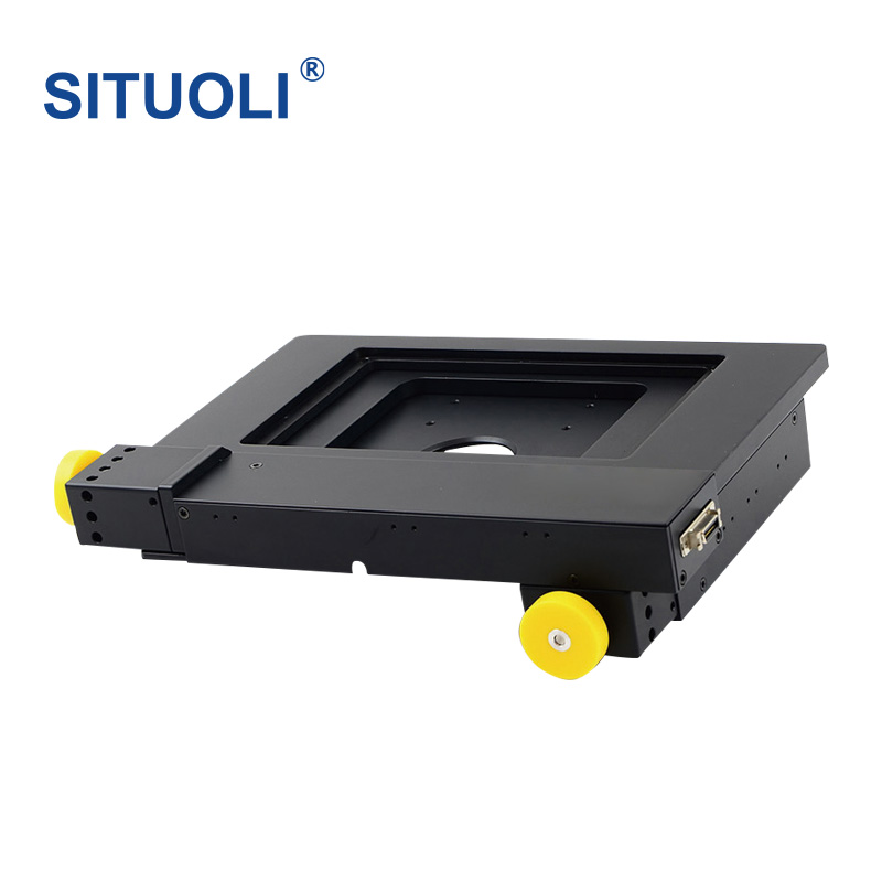 Motorized Stage STL-HSG3000
Motorized Stages
Situoli
Travel Range: 118 mm × 76 mm Travel Speed [4mm ball screw pitch]: Max.150 Repeat Positioning / Repeatability [Bidirectional]: Bidirectional <1
Precision Motorized Microscope Stage for Research,Industry/Biomedicine,Accurate Automatic Movement/Positioning Improves Efficiency/Repeatability,Long Observation,Stitching,Dynamic Samples.
-
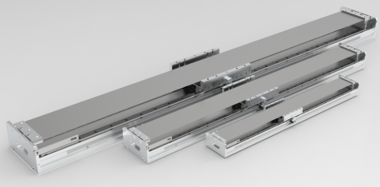 Linear Motor Module STB Series
Motorized Stages
Xzyim
Related Articles
VCSEL, short for Vertical Cavity Surface Emitting Laser, is a widely used semiconductor laser component in modern optoelectronics. Unlike traditional edge-emitting lasers, VCSEL emits laser light vertically from its chip surface. Thanks to its low power consumption, stable beam quality, low cost, and easy integration, it has become the core light source for 3D sensing, wearable devices, and high-speed optical communication.
As fundamental refractive optical components, plano‑convex spherical lenses consist of one convex spherical surface and one flat surface.
FiDAR, the fiber‑optic radar vehicle positioning and tracking system developed by Jianhe Bafang, is a high‑sensitivity distributed fiber‑sensing solution designed for intelligent traffic road monitoring. It outputs real‑time spatial coordinates of every vehicle across the full road section around‑the‑clock, delivering a brand‑new sensing technology for vehicle‑road cooperation, smart highway construction and urban traffic management.
Raybowlaser, a professional manufacturer of high-power laser chips, has officially launched its upgraded new-generation 1470nm high-performance laser chip. Achieving groundbreaking progress in rated output power and wall-plug efficiency (WPE), this innovative laser chip delivers superior and reliable core light source solutions for medical cosmetology, industrial processing, agricultural applications and scientific research equipment.
Loading...
Name
Phone
Organization
Use Case

Database Platform