
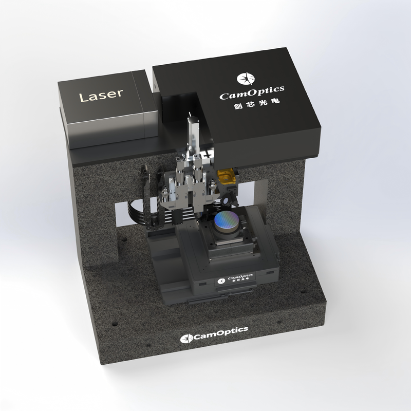
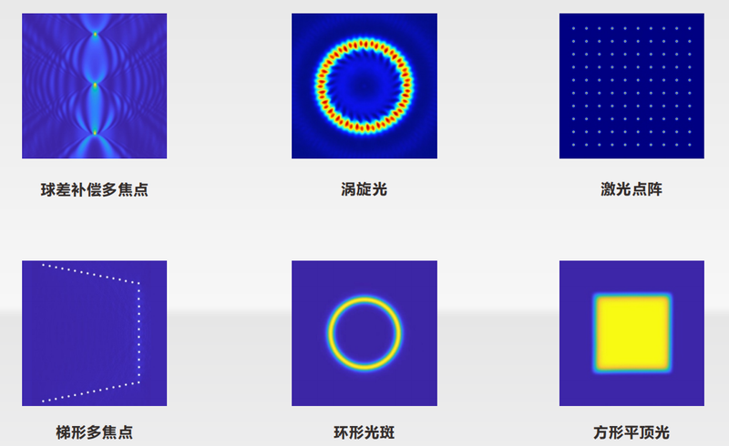



Wafer Stealth-Dicing Optical System Solutions
Jianxin Optoelectronics uses independently developed hologram algorithms to achieve axial multiple foci, transverse multifocus beam splitting, and beam shaping. Applications include ingot separation, wafer stealth dicing, wafer grooving, trapezoidal/C-shaped glass chamfering, metal 3D printing, laser welding, through-holes in lithium battery electrode materials, solar cell scribing, drilling, and other laser processing applications.
 Save to Favorites
Overview
Applications
Key Features
Datasheet
Please provide your email to download the datasheet.
Invalid email format. Please try again.
Supplier Information
Related Products
-
 Laser Manual Center Device
Industrial Manufacturing
Auroralaser
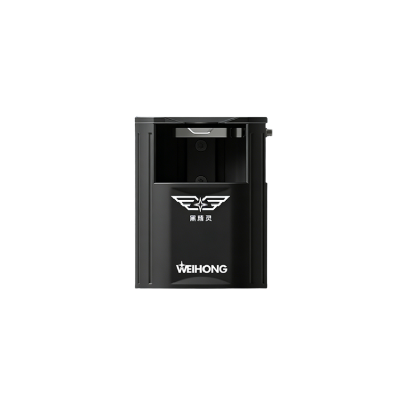
Laser Manual Center Device is designed to improve the coaxiality accuracy between the nozzle and the laser in laser cutting equipment. It achieves rapid and precise adjustment of coaxiality through visual image processing algorithms making it suitable for production scenarios with high requirements for processing accuracy.
-
 Coaxial Linear Nozzle CC-1012(10-15)-01
Industrial Manufacturing
Auroralaser
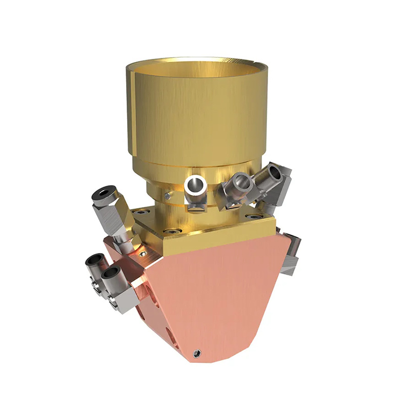
Product Name: Coaxial linear nozzle Type: coaxial Powder flow rate [Same-Name Source Left Column Item Has No Unit; Not Assumed to Be Channel Count]: 2
Transporting strip-shaped powder flow can achieve more efficient laser cladding process on the surface of large workpieces.
-
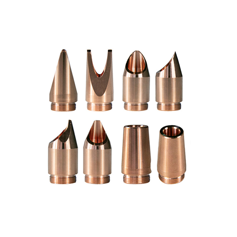 IPG Laser Welding Nozzles
Industrial Manufacturing
Auroralaser
Supply different brands of laser welding nozzles, including IPG, Chaoqiang, Hanwei, Qilin, WSX etc. Other welding spare parts are also available, contact us if you have needs.
-
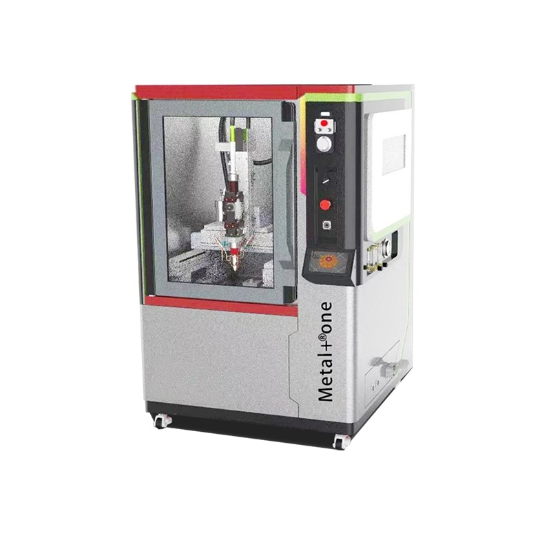 Small Size Metal DED 3D Printing Equipment
Industrial Manufacturing
Auroralaser
Device Name: High throughput metal material 3D printing equipment Scope of work: 300 mm × 300 mm × 200 mm Repetitive displacement accuracy: ±0.05 mm
3D printing high-throughput material equipment that is compact in size, refined and accurate powder feed, especially for use in material design research and laboratory environments. The equipment uses special control software to generate printing tracks and powder feeding rate of each powder bucket for different samples according to different multi-component powder proportion compositions and printing quantity preset in the experiment. When the water and oxygen index in the environmental box is reduced to below 10ppm, printing starts. After the powder with different feeding rate enters the powder mixer for real-time full mixing, it enters the coaxial nozzle under the delivery of inert protective gas and is ejected out. The high-power laser melts the powder and moves according to the preset track driven by the three-axis mechanism to print the test sample blocks with different compositions and proportions.
-
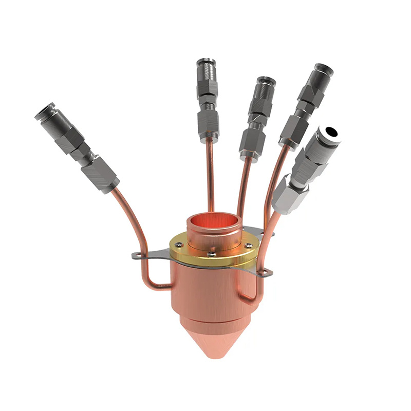 Ordinary Ultrahigh-speed Coaxial Annular Nozzle CF-0406-01
Industrial Manufacturing
Auroralaser
Product Name: Ordinary ultra high speed coaxial annular nozzle Material: Red copper Laser power: ≤3 KW
Ordinary super-high speed laser cladding nozzle is customized for precision workpiece, and copper material with high heat dissipation performance is selected. Fine powder discharge can easily form dense coating and microstructure, which is suitable for cladding with high forming accuracy.
Related Articles
VCSEL, short for Vertical Cavity Surface Emitting Laser, is a widely used semiconductor laser component in modern optoelectronics. Unlike traditional edge-emitting lasers, VCSEL emits laser light vertically from its chip surface. Thanks to its low power consumption, stable beam quality, low cost, and easy integration, it has become the core light source for 3D sensing, wearable devices, and high-speed optical communication.
As fundamental refractive optical components, plano‑convex spherical lenses consist of one convex spherical surface and one flat surface.
FiDAR, the fiber‑optic radar vehicle positioning and tracking system developed by Jianhe Bafang, is a high‑sensitivity distributed fiber‑sensing solution designed for intelligent traffic road monitoring. It outputs real‑time spatial coordinates of every vehicle across the full road section around‑the‑clock, delivering a brand‑new sensing technology for vehicle‑road cooperation, smart highway construction and urban traffic management.
Raybowlaser, a professional manufacturer of high-power laser chips, has officially launched its upgraded new-generation 1470nm high-performance laser chip. Achieving groundbreaking progress in rated output power and wall-plug efficiency (WPE), this innovative laser chip delivers superior and reliable core light source solutions for medical cosmetology, industrial processing, agricultural applications and scientific research equipment.
Loading...
Name
Phone
Organization
Use Case

Database Platform