
10G Intensity modulator JDSU X5/Z5
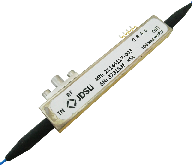
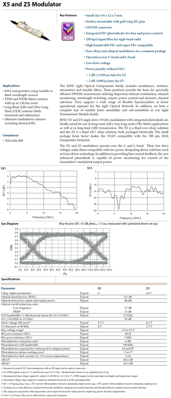
The X5 and Z5 are 10Gbps intensity modulators,single GPO RF port;4.5dB low insertion loss,extinction ratio greater than 30dB,extinction ratio can exceed 40dB or 50dB,low drive voltage.The biggest difference is that the latter has fixed chirp. JDSU X5 and Z5 single drive 10 Gb/s modulators with integrated photodiode are ideally suited for use in long reach (LR)/very long reach (VR) Metro applications as well as in long haul (LH) transmission. The X5 is a fixed zero-chirp solution and the Z5 is a fixed ±0.7 chirp solution, both packaged identically. The small package form factor makes the X5/Z5 compatible with the 300 pin MSA transponder footprint. The X5 and Z5 modulators operate over the C and L band. Their low drive voltages make them compatible with low power dissipating driver solutions such as GaAs driver technology. In addition to providing bias control feedback, the new enhanced photodiode is capable of power monitoring for control of the transmitter’s modulated output power.
 Save to Favorites
Overview
Specifications
| Parameter | Value |
|---|---|
| Chirp (alpha parameter) | typical: ±0.7 |
| Optical insertion loss (BOL) [Measured at peak of DC bias transmission with no RF input and no optical connectors.] | typical:4.5 dB |
| Optical return loss (input and output ports) | typical:40 dB |
| Optical on/off extinction ratio [Low frequency] | typical:27 dB |
| Optical on/off extinction ratio [PRBS / For PRBS signals of up to 2³¹−1 and at bit rates up to 12.5 Gb/s. Measurement is based on an optimized set up.] | typical:15 dB |
| E/O bandwidth [-3 dB electrical, linear fit 2 to 15 GHz] | typical:12 GHz |
| S11 (130 MHz to 10 GHz) | typical:10 dB |
| Drive voltage (RF port) [Maximum driving voltage required to achieve 15 dB ER for 12.5 Gb/s 2³¹−1 PRBS signal over the operating wavelength and temperature ranges.] | typical:4.5 V |
| Vπ bias port [40 kHz] | typical:2.5 V |
| Bias voltage range [Maximum voltage range required to maintain optimum bias point over life and temperature.] | typical:-15 to 15 V |
| RF port resistance [DC] | typical:40 Ω |
| Bias port resistance [DC] | typical:1 MΩ |
| Photodetector extinction ratio [ER=10*log(Imax/Imin): Imax=PD current with modulator biased to maximum output power, Imin=PD current with modulator biased to minimum output power.] | typical:6 dB |
| Photodetector O/E bandwidth | typical:100 kHz |
| Photodetector responsivity [referred to output power] | typical:20 mA/W |
| Photodetector phase tracking error [Tracking error is the difference in phase between the modulator output power transfer function and the photodetector output current transfer function.] | typical:-5 to 5° |
| Photodetector dark current [at -5 V, room temperature] | typical:5 nA |
| ΔR/ΔT [The change in responsivity with temperature can be improved from the values given by employing passive thermal compensation.] | typical:±0.2 dB |
| ΔR/Δλ [Over C or L band. This can be calibrated for a given laser frequency.] | typical:±0.3 dB |
Applications
Key Features
Datasheet
Please provide your email to download the datasheet.
Invalid email format. Please try again.
Supplier Information
Related Products
-
 Large-Aperture Pockels Cell GPC-001
EOM
Gigaphotonics
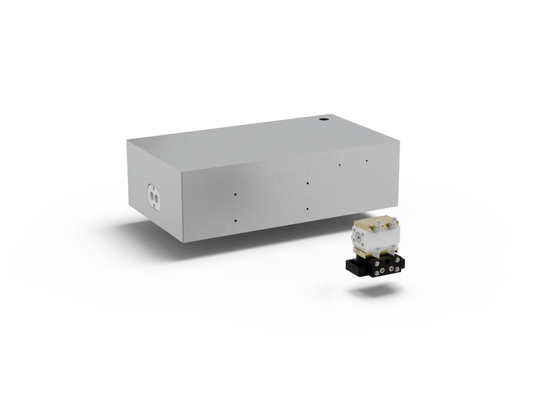
Maximum Repetition Rate: 1 kHz Wavelength and Damage Threshold [10ns; 10 Hz]: 1030 nm,10 J/cm², 10ns, 10 Hz Crystal Quantity: Single BBO or Dual BBO Crystal
A Pockels cell uses phase retardation in an electro-optic crystal: applied voltage provides electro-optic modulation or switching. It is a core component of Q-switched lasers and regenerative amplifiers. GPC Pockels cells offer a large clear aperture, high-voltage/high-repetition-rate modulation, compact size and easy optical adjustment. Host-computer software lets researchers adjust parameters and display status in real time.
-
 Large-Aperture Pockels Cell GPC-010
EOM
Gigaphotonics
Maximum Repetition Rate: 10 kHz Wavelength and Damage Threshold [10ns; 10 Hz]: 1030 nm,10 J/cm², 10ns, 10 Hz Crystal Quantity: Single BBO or Dual BBO Crystal
A Pockels cell uses phase retardation in an electro-optic crystal: applied voltage provides electro-optic modulation or switching. It is a core component of Q-switched lasers and regenerative amplifiers. GPC Pockels cells offer a large clear aperture, high-voltage/high-repetition-rate modulation, compact size and easy optical adjustment. Host-computer software lets researchers adjust parameters and display status in real time.
-
 Large-Aperture Pockels Cell GPC-100
EOM
Gigaphotonics
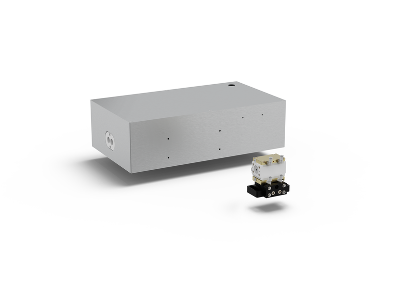
Maximum Repetition Rate: 100 kHz Wavelength and Damage Threshold [10ns; 10 Hz]: 1030 nm,10 J/cm², 10ns, 10 Hz Crystal Quantity: Single BBO or Dual BBO Crystal
A Pockels cell uses phase retardation in an electro-optic crystal: applied voltage provides electro-optic modulation or switching. It is a core component of Q-switched lasers and regenerative amplifiers. GPC Pockels cells offer a large clear aperture, high-voltage/high-repetition-rate modulation, compact size and easy optical adjustment. Host-computer software lets researchers adjust parameters and display status in real time.
-
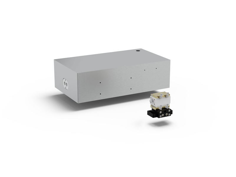 Large-Aperture Pockels Cell GPC-500
EOM
Gigaphotonics
Maximum Repetition Rate: 500 kHz Wavelength and Damage Threshold [10ns; 10 Hz]: 1030 nm,10 J/cm², 10ns, 10 Hz Crystal Quantity: Single BBO or Dual BBO Crystal
A Pockels cell uses phase retardation in an electro-optic crystal: applied voltage provides electro-optic modulation or switching. It is a core component of Q-switched lasers and regenerative amplifiers. GPC Pockels cells offer a large clear aperture, high-voltage/high-repetition-rate modulation, compact size and easy optical adjustment. Host-computer software lets researchers adjust parameters and display status in real time.
-
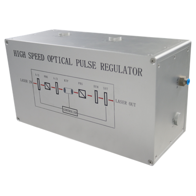 Pockels Cell-1030 High-Speed Laser Pulse Optical Switching Module
EOM
Unityphotonics
Operating voltage: 3kV Max Repetition Rate: 1MHz Leading and trailing edges: <10ns
Related Articles
Macro channel water-cooled stacked laser diodes integrate dozens of laser bars into one vertical stacked module with large-diameter macro flow cooling channels.
Fomoptic delivers integrated one‑stop optical solutions covering precision optical fabrication and custom vacuum coating services. Supported by complete processing production lines, comprehensive metrology equipment and experienced engineering team, we provide full‑chain customized components, ranging from blank shaping, ultra‑precision polishing to thin‑film coating, for laser systems, infrared imaging, industrial optics and scientific‑research projects.
The accelerated construction of new‑generation power systems has brought revolutionary upgrades to power‑equipment maintenance workflows.
The MSL‑T series water‑cooled continuous‑wave single‑longitudinal‑mode lasers from Changchun New Industries Optoelectronics (CNI) deliver key research wavelengths including 369 nm, 405 nm and 770 nm.
Loading...
Name
Phone
Organization
Use Case

Database Platform