

ZnSe+Cr:ZnSe+ZnSe
Our ZnSe+Cr:ZnSe+ZnSe bonded crystal is formed by bonding pure ZnSe to both ends of Cr:ZnSe, effectively improving the overall performance of the Cr:ZnSe laser. The thermal conductivity of Cr:ZnSe is 14W/cm/°K@20°C, and that of ZnSe is 18W/m/K. Bonding the two ends to form ZnSe+Cr:ZnSe+ZnSe reduces thermal effects in Cr:ZnSe, decreases thermal lensing during laser pumping, improves beam quality, increases output stability and extends laser service life. Other advantages include broad tunability (emission from 2.1-3.1μm), a larger gain cross section (σ emission ~9 × 10⁻¹⁹ cm²), and minimal excited-state absorption because spin transitions to upper excited states are forbidden. Crylink uses surface-activated bonding, a bonding technology performed at low or room temperature and characterized by surface cleaning and activation. Bombardment of the bonding surfaces with fast atoms or an ion beam before bonding effectively increases bonding strength and enables high-quality bonding between inorganic materials, metals and semiconductor materials. Compared with high-temperature thermal bonding, surface-activated bonding provides greater interfacial bonding strength and better control of optical absorption loss and surface-figure change. Impurities on thermally diffusion-bonded surfaces cannot be removed and remain trapped at the bonded interface. Surface-activated bonding can remove polishing residues, organic contamination and surface oxide layers, break material chemical bonds and increase activation energy. The manufactured ZnSe+Cr:ZnSe+ZnSe bonded crystals have high bond strength, low absorption loss at the bonded interface (generally below 20ppm), and small surface-figure changes at the interface (surface figure <lamda/8 after bonding). They can be made as rods, slabs, waveguides or sandwich structures. Various coatings are available on the two ends, such as AR@2300~2500nm on the end faces. ZnSe+Cr:ZnSe+ZnSe bonded crystals are widely used in optical communication, pollutant-gas detection and industrial combustion-product testing.
 Save to Favorites
Overview
Specifications
| Parameter | Value |
|---|---|
| concentrations [Materials:Cr:ZnSe] | (1~9)*10¹⁸/cm³ |
| Structure [Materials:ZnSe / Structure;Cr:ZnSe:Rods/Slabs/Sandwich/Waveguide/ / Structure;ZnSe:Rods/Slabs/Sandwich/Waveguide/] | Rods/Slabs/Sandwich/Waveguide/ |
| Structure [Materials:Cr:ZnSe / Structure;ZnSe:Rods/Slabs/Sandwich/Waveguide/] | Rods/Slabs/Sandwich/Waveguide/ |
| Structure [Materials:ZnSe / Structure;ZnSe:Rods/Slabs/Sandwich/Waveguide/ / Structure;Cr:ZnSe:Rods/Slabs/Sandwich/Waveguide/] | Rods/Slabs/Sandwich/Waveguide/ |
| End-face Configuration [Materials:ZnSe / End-face Configuration;Cr:ZnSe:Flat/Convex/Wedge / End-face Configuration;ZnSe:Flat/Convex/Wedge] | Flat/Convex/Wedge |
| End-face Configuration [Materials:Cr:ZnSe / End-face Configuration;ZnSe:Flat/Convex/Wedge] | Flat/Convex/Wedge |
| End-face Configuration [Materials:ZnSe / End-face Configuration;ZnSe:Flat/Convex/Wedge / End-face Configuration;Cr:ZnSe:Flat/Convex/Wedge] | Flat/Convex/Wedge |
| Side Configuration [Materials:ZnSe / Side Configuration;Cr:ZnSe:Polish/Fine Ground / Side Configuration;ZnSe:Polish/Fine Ground] | Polish/Fine Ground |
| Side Configuration [Materials:Cr:ZnSe / Side Configuration;ZnSe:Polish/Fine Ground] | Polish/Fine Ground |
| Side Configuration [Materials:ZnSe / Side Configuration;ZnSe:Polish/Fine Ground / Side Configuration;Cr:ZnSe:Polish/Fine Ground] | Polish/Fine Ground |
| Coating available [Materials:ZnSe / Coating available;ZnSe:AR@2300~2500nm / @2300~2500nm] | AR@2300~2500nm |
Datasheet
Supplier Information
Related Products
-
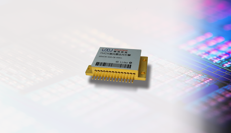 Silicon Photonics Transmit/Receive Integrated Optical Engine
Optical Material
Inxuntech
Yingxun Xinguang's silicon-photonics integrated transceiver optical-engine module includes integrated transmission/reception with laser and receiver, tunable photonics for fast response and wide dynamic range, multiwavelength Mux/DeMux with no moving parts and high reliability, and hybrid III-V/silicon integration for high performance and compact size.
-
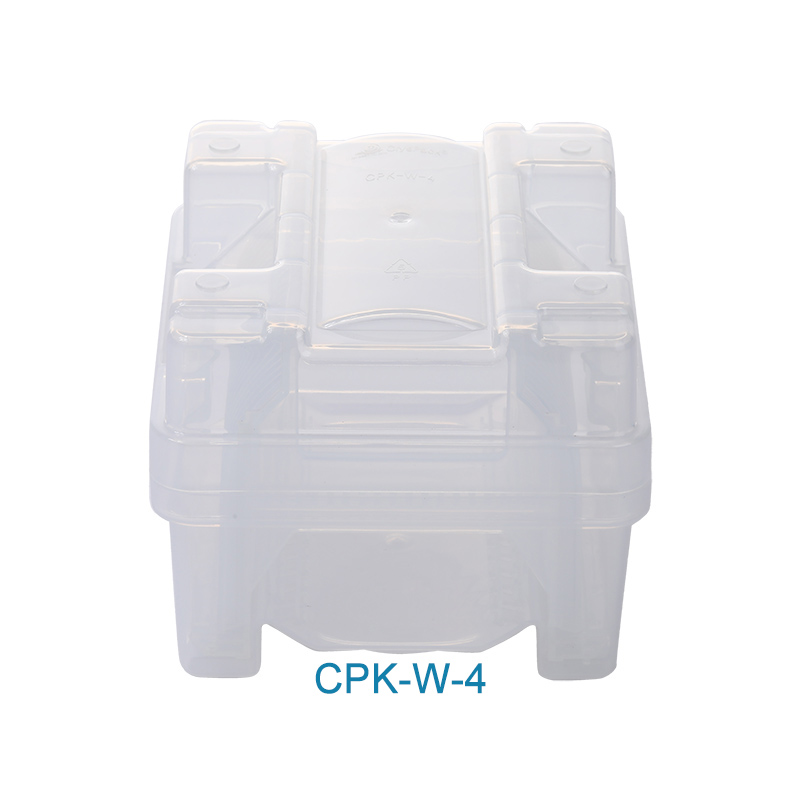 4-Inch Silicon Wafer Carrier
Optical Material
Cryspack
The 4-inch silicon-wafer carrier packages, stores, transfers or displays precision devices and stores, transfers and transports wafers and circular thin sheets. See this page's specifications for dimensions, materials and structure. Contact Kangpaike to confirm samples, specifications, materials or customization.
-
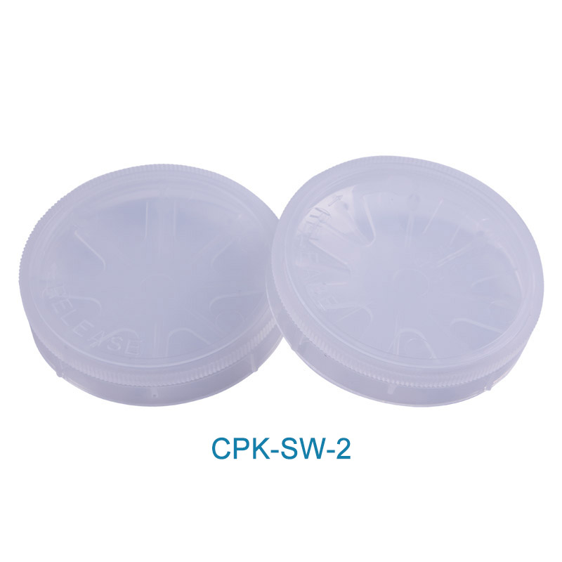 Single Silicon Wafer Carrier Box
Optical Material
Cryspack
The single-silicon-wafer carrier box packages, stores, transfers or displays precision devices and stores, transfers and transports wafers and circular thin sheets. See this page's specifications for dimensions, materials and structure. Contact Kangpaike to confirm samples, specifications, materials or customization.
-
 Silicon Wafer Vacuum-Holding Box
Optical Material
Cryspack
The silicon-wafer vacuum holding box packages, stores, transfers or displays precision devices. It is suitable for holding, transferring and releasing precision semiconductor devices. See this page's specifications for dimensions, materials and structure. Contact Kangpaike to confirm samples, specifications, materials or customization.
-
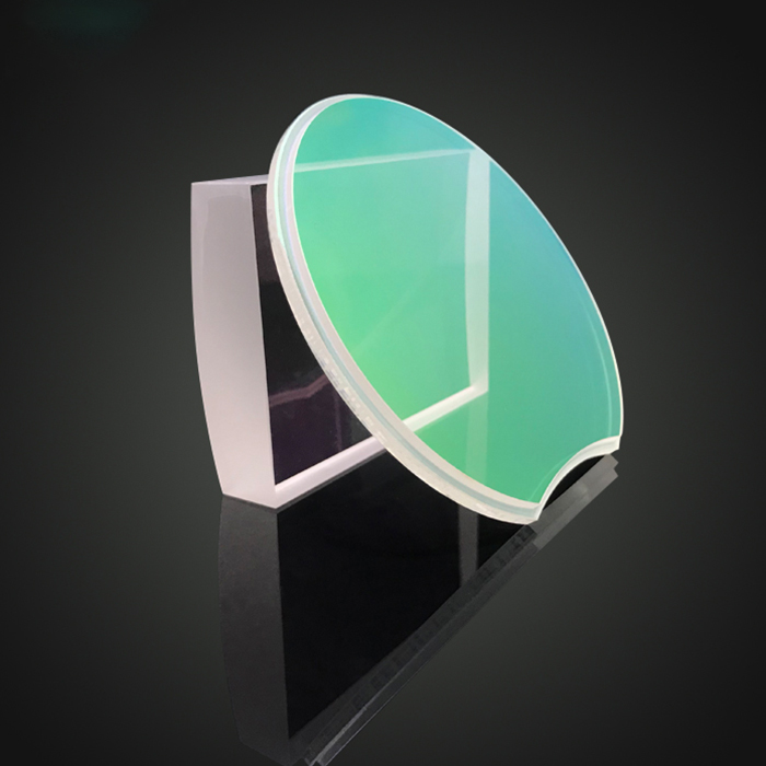 N-BK7 Window
Optical Material
Sunday-optics
Diameter: 1 mm to 1000 mm Diameter Tolerance: +/-0.02 mm Material: Bk7 Sapphire Fused silica 、ZnS2、CaF2、Si、Ge。
Sunday-optics specializes in precision optical windows, using four-axis polishers, large annular polishers and two-axis machines to manufacture high-precision windows for customers.
Related Articles
Macro channel water-cooled stacked laser diodes integrate dozens of laser bars into one vertical stacked module with large-diameter macro flow cooling channels.
Fomoptic delivers integrated one‑stop optical solutions covering precision optical fabrication and custom vacuum coating services. Supported by complete processing production lines, comprehensive metrology equipment and experienced engineering team, we provide full‑chain customized components, ranging from blank shaping, ultra‑precision polishing to thin‑film coating, for laser systems, infrared imaging, industrial optics and scientific‑research projects.
The accelerated construction of new‑generation power systems has brought revolutionary upgrades to power‑equipment maintenance workflows.
The MSL‑T series water‑cooled continuous‑wave single‑longitudinal‑mode lasers from Changchun New Industries Optoelectronics (CNI) deliver key research wavelengths including 369 nm, 405 nm and 770 nm.
Loading...
Name
Phone
Organization
Use Case

Database Platform