
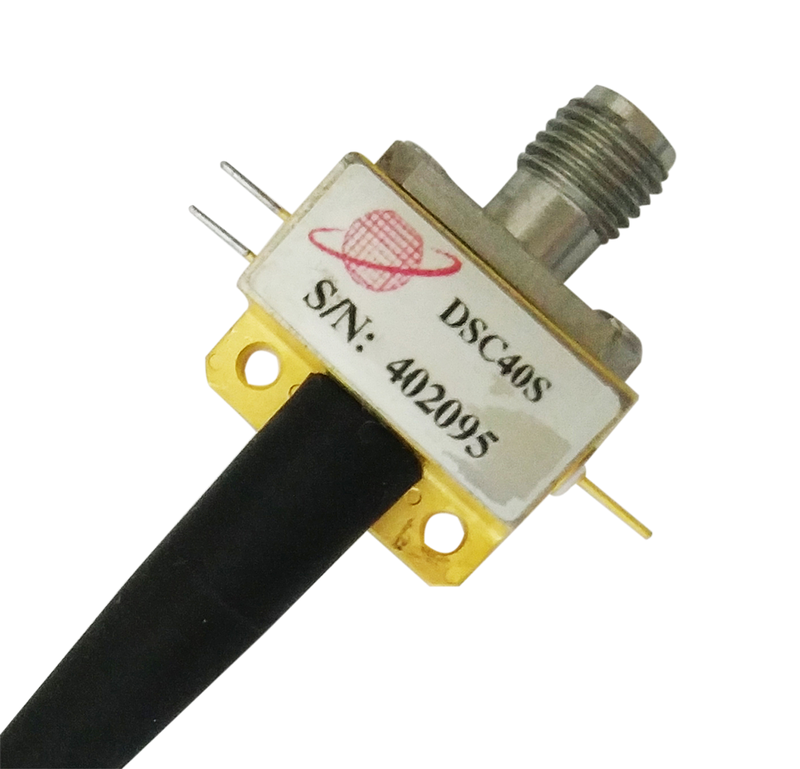
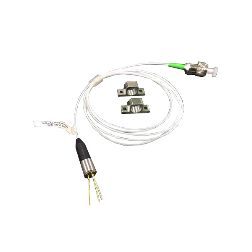
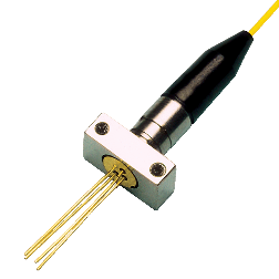
14G Photodetector Analog PIN Photodetector Discovery DSC40S
The photodetector with fiber tails input,3dB typical bandwidth 16GHz,can be used for microwave photon communication;RF SMA/K port,low distortion,linear PIN,analog detector, ultra wide working band 800~1650nm,wide response range,has an optical input power damage threshold of +17dBm for NRZ with 50% duty cycle,response degree 0.8A/W. These high speed photodiodes are hermetically sealed, high reliability, low harmonic distortion photodiode modules designed for high optical power applications with typical bandwidths of 16GHz, respectively. The devices are well suited for receiver applications with optical pre-amplification, and are available with an internal 50 Ω termination. These photodiode modules are available in a K-connector package RF output, and utilize Discovery’s high-reliability InGaAs photodiode technology.
 Save to Favorites
Overview
Specifications
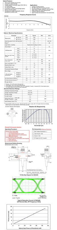
| Parameter | Value |
|---|---|
| Responsivity [Source technical matrix with literal variant labels50S/40S/30S; complete added model codes not supplied / @1550nm] | min:0.65 A/W;typical:0.80 A/W |
| Responsivity [Source technical matrix with literal variant labels50S/40S/30S; complete added model codes not supplied / @1310nm] | min:0.70 A/W;typical:0.80 A/W |
| Noise Equivalent Power (NEP) [Source technical matrix with literal variant labels50S/40S/30S; complete added model codes not supplied / @300K] | typical:22 pW/√HZ |
| Ripple [Source technical matrix with literal variant labels50S/40S/30S; complete added model codes not supplied / Flatness—DC to70% of the3dB bandwidth.] | typical:+/-1 |
| Logic Sense / Coupling [Source technical matrix with literal variant labels50S/40S/30S; complete added model codes not supplied] | Positive Non-Inverting / DC50Ω |
| Group Delay [Source technical matrix with literal variant labels50S/40S/30S; complete added model codes not supplied / Group Delay—DC to70% of the3dB bandwidth.] | typical:±7 ps |
| 3dB Bandwidth [Source table variant 50S (literal short label) / Power Bandwidth of unterminated50,40 &30 is unspecified: Typically, it measures50% of terminated version.] | min:10 GHz;typical:12 GHz |
| 3dB Bandwidth [Source table variant 40S (literal short label) / Power Bandwidth of unterminated50,40 &30 is unspecified: Typically, it measures50% of terminated version.] | min:14 GHz;typical:16 GHz |
| 3dB Bandwidth [Source table variant 30S (literal short label) / Power Bandwidth of unterminated50,40 &30 is unspecified: Typically, it measures50% of terminated version.] | min:18 GHz;typical:22 GHz |
| Rise Time [Source table variant 50S; original ordered heading Rise Time/Fall Time/FWHM and ordered tuple 17, 23, 30] | typical:17 ps |
| Fall Time [Source table variant 50S; original ordered heading Rise Time/Fall Time/FWHM and ordered tuple 17, 23, 30] | typical:23 ps |
| FWHM [Source table variant 50S; original ordered heading Rise Time/Fall Time/FWHM and ordered tuple 17, 23, 30] | typical:30 ps |
| Rise Time [Source table variant 40S; original ordered heading Rise Time/Fall Time/FWHM and ordered tuple 15, 18, 25] | typical:15 ps |
| Fall Time [Source table variant 40S; original ordered heading Rise Time/Fall Time/FWHM and ordered tuple 15, 18, 25] | typical:18 ps |
| FWHM [Source table variant 40S; original ordered heading Rise Time/Fall Time/FWHM and ordered tuple 15, 18, 25] | typical:25 ps |
| Rise Time [Source table variant 30S; original ordered heading Rise Time/Fall Time/FWHM and ordered tuple 14, 16, 22] | typical:14 ps |
| Fall Time [Source table variant 30S; original ordered heading Rise Time/Fall Time/FWHM and ordered tuple 14, 16, 22] | typical:16 ps |
| FWHM [Source table variant 30S; original ordered heading Rise Time/Fall Time/FWHM and ordered tuple 14, 16, 22] | typical:22 ps |
| Power Dissipation V_bd*I_bd [Source table variant 50S,40S] | max:200 mW |
| Power Dissipation V_bd*I_bd [Source table variant 30S] | max:150 mW |
| Dark Current [Source technical matrix with literal variant labels50S/40S/30S; complete added model codes not supplied / @25°C,5V] | typical:10 nA;max:100 nA |
| Electrical Return Loss [Source technical matrix with literal variant labels50S/40S/30S; complete added model codes not supplied] | typical:-10 dB |
| Optical Return Loss [Source technical matrix with literal variant labels50S/40S/30S; complete added model codes not supplied] | min:27 dB;typical:30 dB |
| Wavelength Response Range [Source technical matrix with literal variant labels50S/40S/30S; complete added model codes not supplied] | min:1064 nm;max:1650 nm |
| Bias Voltage [Source technical matrix with literal variant labels50S/40S/30S; complete added model codes not supplied] | typical:+5 V;max:+7 V |
| 1dB small signal compression [Source table variant 50S / @5V] | typical:20 mA;max:28 mA |
| 1dB small signal compression [Source table variant 40S / @5V] | typical:18 mA;max:26 mA |
| 1dB small signal compression [Source table variant 30S / @5V] | typical:16 mA;max:23 mA |
| 2nd Order Harmonic Distortion [Source technical matrix with literal variant labels50S/40S/30S; complete added model codes not supplied / At+4dBm Optical Power and5.8GHz Fundamental.] | min:-70 dBc |
| 3rd Order Harmonic Distortion [Source technical matrix with literal variant labels50S/40S/30S; complete added model codes not supplied / At+4dBm Optical Power and5.8GHz Fundamental.] | min:-75 dBc |
| PDL [Source technical matrix with literal variant labels50S/40S/30S; complete added model codes not supplied / @1550nm] | typical:0.05 dB;max:0.12 dB |
| Operating Temperature Range [Absolute Maximum Ratings / Source technical matrix with literal variant labels50S/40S/30S; complete added model codes not supplied] | 0 to+70 °C |
| Storage Temperature Range [Absolute Maximum Ratings / Source technical matrix with literal variant labels50S/40S/30S; complete added model codes not supplied] | -40 to+85 °C |
| PIN Bias Voltage [Absolute Maximum Ratings / Source technical matrix with literal variant labels50S/40S/30S; complete added model codes not supplied] | +0.5 to+7 V |
| Forward Current [Absolute Maximum Ratings / Source technical matrix with literal variant labels50S/40S/30S; complete added model codes not supplied] | 10 mA |
| Optical Input Power Damage Threshold [Absolute Maximum Ratings / Source table variants50S,40S / Assumes NRZ with50% duty cycle. Peak RZ or narrow pulse width will hit peak limit at lower average optical input powers than observed with50% duty cycle data.] | +17 dBm |
| Optical Input Power Damage Threshold [Absolute Maximum Ratings / Source table variant30S / Assumes NRZ with50% duty cycle. Peak RZ or narrow pulse width will hit peak limit at lower average optical input powers than observed with50% duty cycle data.] | +16 dBm |
| Lead Soldering Temp [Absolute Maximum Ratings / 10s] | 250 °C |
Applications
Key Features
Datasheet
Please provide your email to download the datasheet.
Invalid email format. Please try again.
Supplier Information
Related Products
-
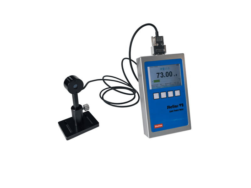 Stellar-PD300C,PD300C-1.5W,PD300C-3W,PD300C-UV0 Photodiode Laser Power Meter
Photodiodes
Shafan-oe
Meter Head-Power-Supply Method: USB-B interface, 5V1A phone charger Meter Head-Battery Characteristics: 3800MAH; charging time 10 hours; discharge time 24 hours Meter Head - Display: 3.5-inch true-color LCD, 480*320, multi-level backlight
LCD with Chinese/English interface; pW~W power measurement; wavelength coverage 250nm-1800nm; automatic and manual ranging; NIST traceability; convenient self-calibration; optional fiber adapters (ST, FC, LC, SC); compact design and rotating stand for easy placement
-
 50um Indium Gallium Arsenide Avalanche Photodiode OAPD-X-X-P-XX-X
Photodiodes
O-send
Absolute Maximum Ratings - Storage Temperature: -55°C~+85°C Absolute Maximum Ratings - Operating temperature: -40°C~+85°C Absolute Maximum Ratings-Reverse Current [CW]: 3mA
The 50um InGaAs APD pigtail module is widely used in OTDR, CATV and optical repeater equipment.
-
 75um Indium Gallium Arsenide Photodiode OPD-1-X-X-X-XX-X-X
Photodiodes
O-send
Absolute Maximum Ratings - Storage Temperature: -40°C~+100°C Absolute Maximum Ratings - Operating temperature: -40°C~+85°C Absolute Maximum Ratings - Reverse Voltage [CW]: 30V
75um InGaAs photodiodes are widely used in cable television optical reception, analog transmission, optical communications and test instruments.
-
 InGaAs Photo Diode OAPD-X-X-P-XX-X
Photodiodes
O-send
21°C General Characteristics at - Wavelength Range [1550nm( Type )]: min:1100 nm;max:1650 nm General Characteristics at 21°C-Peak Sensitivity: 1550nm 21°C General Characteristics at - Storage Temperature: 60°C~125°C
This product is suitable for ranging optics, communication systems, optical coherence tomography and low-light detection. Sizes of 80um, 200um and 300um are available. Peak responsivity occurs at 1550nm.
-
 Silicon Avalanche Photodiode OAPD-2-X-X-X-XX-X
Photodiodes
O-send
Detection Range: 400~1100nm Dark current: typical:0.2 Responsivity: min:0.40 A/W;typical:0.55 A/W
The fiber-coupled silicon avalanche photodiode couples to single-mode or multimode fiber. Various active diameters are available, including 200um and 500um. It is commonly used in telecommunications, data communications, optical communications, test instruments and OTDR.
Related Articles
Semiconductor laser diodes are essential light sources for industrial sensing, LiDAR and laser printing. Many engineers waste time picking mismatched models. We summarize 4 simple selection standards, plus a mature industrial product: HGLD-790TO5.6-ZSP-10mW from HAUCORE.
Polycom Photonics Co., Ltd focuses on the R&D and mass production of high-stability, narrow-linewidth laser sources for optical sensing applications. The company provides cost-effective and high-precision optical sensing lasers with a wavelength coverage from 689nm to 2350nm. Featuring accurate wavelength control and outstanding spectral stability, these laser products are widely applied in atomic spectrum detection, element precision measurement and professional optoelectronic sensing systems.
As a professional manufacturer of precision optical thin-film components, sycco-optics (Shandong Yanggu Hengjing Optoelectronics) launches high-performance 850nm narrow band pass filters for near-infrared precision detection, intelligent sensing and optical imaging systems. Adopting advanced vacuum coating technology, the filter realizes high transmittance in the target band and deep blocking in interference bands. It effectively eliminates stray light and spectral noise, serving as a core optical component for machine vision, biochemical detection and photoelectric sensing equipment.
FiDAR, the fiber‑optic radar vehicle positioning and tracking system developed by Jianhe Bafang, is a high‑sensitivity distributed fiber‑sensing solution designed for intelligent traffic road monitoring. It outputs real‑time spatial coordinates of every vehicle across the full road section around‑the‑clock, delivering a brand‑new sensing technology for vehicle‑road cooperation, smart highway construction and urban traffic management.
Loading...
Name
Phone
Organization
Use Case

Database Platform