
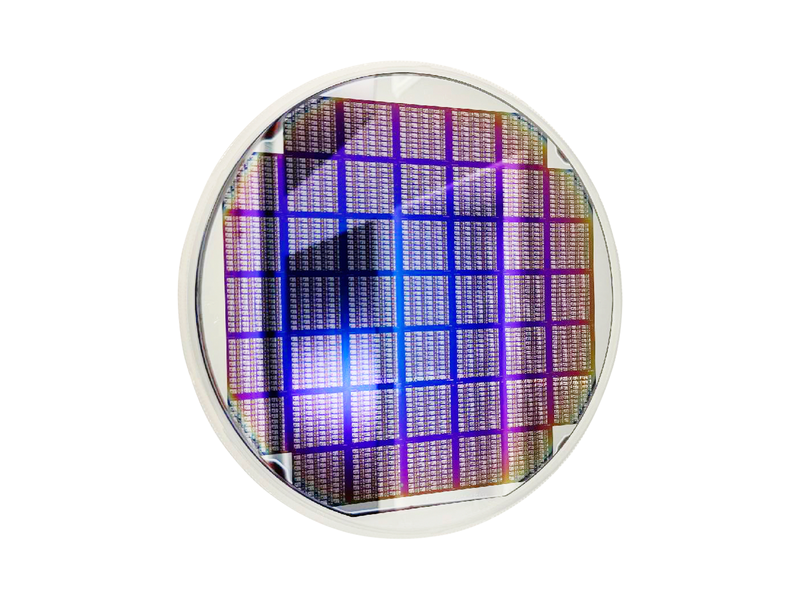

Silicon photomultiplier
A SiPM (silicon photomultiplier, also called a multipixel photon counter, MPPC) is an array of hundreds to tens of thousands of identical Geiger-Avalanche Photodiode (G-APD) cells, each approximately 1~100 μm in diameter, integrated in parallel on a monocrystalline silicon chip. Each cell is connected in series with a resistor of hundreds of kilohms to quench the large avalanche current promptly. All cells share a signal electrode and operate in Geiger mode, several volts above the cell breakdown voltage. Each silicon photomultiplier consists of many hundreds or thousands of APD cells, each comprising an APD in series with a high-value quenching resistor, connected in parallel as an area array. With reverse bias, generally tens of volts, a strong electric field forms in each APD depletion region. The source offers the simplified, explicitly imprecise explanation that an incoming photon undergoes Compton scattering with electron-hole pairs, releasing an electron or hole. High-energy carriers accelerate in the field and create many secondary carriers, producing an avalanche. The resulting increase in cell current increases the voltage drop across quenching resistor R and rapidly lowers the APD field, stopping the avalanche after a transient current pulse. Equal quenching resistances mean that cells theoretically produce equal pulses. Although APDs are analog devices, each cell behaves macroscopically as a logic element: output is “1” when a signal is present and “0” otherwise. Within the SiPM dynamic range, output current is proportional to the number of cells undergoing avalanches.
 Save to Favorites
Overview
Specifications
| Parameter | Value |
|---|---|
| Spectral response range λ | 320 to ~900 |
| Peak sensitivity wavelength λp [Depends on the die model] | 360~470( Depends on the die model ) |
| Temperature for stable signal output [Ta=25℃±10℃] | typical:±5 % |
| Photosensitivity Rv | min:2.1×10⁶;typical:2.6×10⁶;max:3.2×10⁶ |
| Rise Time | typical:2 ns |
| Photoresponse pulse FWHM | typical:4 ns |
| Photon counting frequency fc | max:80 MHz |
| Dark count rate (at recommended bias) DCR | typical:~400 KHz |
| Noise Equivalent Power NEP [Complete darkness] | typical:3 fw/Hz1/2 |
| Number of resolved photons for pulsed light (average) PNR | min:0.1 units;typical:20 units;max:47 units |
| Saturating incident optical flux Pin | typical:~100 nW |
Applications
Key Features
Datasheet
Supplier Information
Related Products
-
 PD-500B
Optical Detectors
Inxuntech
Center wavelength: 800~1700nm Bandwidth (3dB): 500MHz Common-Mode Rejection Ratio: >25dB
Yingxun Xinguang's balanced photodetection module combines precision symmetrical optics, matched high-frequency InGaAs photodiodes and an ultra-low-noise transimpedance amplifier (TIA). This high-performance module provides high bandwidth and excellent common-mode noise rejection.
-
 Whisper Silicon Solid-State Detector Module
Optical Detectors
Pavilionintegration
Input Supplier Voltage: +/-5V Photoelectric Sensitivity [Typical]: 6.0x10⁷ V/W(Typical) Effective Sensing Srea: Ф1/Ф3mm
As the semiconductor industry advances, solid-state detectors (SSDs), including silicon photomultipliers (SiPMs) and other semiconductor photodetectors, are developing rapidly. Heat-dissipation modules, PCBs, special optics and other functional modules can be added to their configuration for fluorescence detection in life-science instruments, providing excellent performance and reliability. Used together with PIC's innovative, compact, low-noise diode lasers, SiPM detectors support clinical, diagnostic and research applications in moving toward smaller, highly integrated and highly reliable systems.
-
 Whisper Silicon Solid-State Detector Module
Optical Detectors
Pavilionintegration
Input Supplier Voltage: +/-5V Photoelectric Sensitivity [Typical]: 6.0x10⁷ V/W(Typical) Effective Sensing Srea: Ф1/Ф3mm
As the semiconductor industry advances, solid-state detectors (SSDs), including silicon photomultipliers (SiPMs) and other semiconductor photodetectors, are developing rapidly. Heat-dissipation modules, PCBs, special optics and other functional modules can be added to their configuration for fluorescence detection in life-science instruments, providing excellent performance and reliability. Used together with PIC's innovative, compact, low-noise diode lasers, SiPM detectors support clinical, diagnostic and research applications in moving toward smaller, highly integrated and highly reliable systems.
-
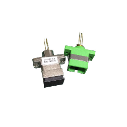 1000um Indium Gallium Arsenide Detector OPD-1-X-X-X-XX-X
Optical Detectors
O-send
Absolute Maximum Ratings - Storage Temperature: -40°C~+100°C Absolute Maximum Ratings - Operating temperature: -40°C~+85°C Absolute Maximum Ratings - Reverse Voltage [CW]: 30V
The 1000um InGaAs detector is mainly used to manufacture power meters. Its detection wavelength ranges from 800nm to 1700nm, and its photosensitive area is 1000um.
-
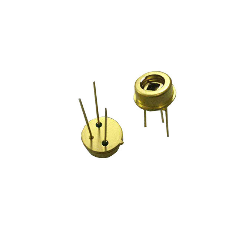 2000um Indium Gallium Arsenide Detector Die OTC-PD-2000-TOXX-XX
Optical Detectors
O-send
Responsivity [Vr=-5V]: min:0.70;typical:0.85 Dark current: max:0.7 mA Photosensitive Area Diameter: 2000um
2000μm InGaAs PIN detectors in TO-CAN packages are widely used in the manufacture of optical communication, test and measurement equipment.
Related Articles
Semiconductor laser diodes are essential light sources for industrial sensing, LiDAR and laser printing. Many engineers waste time picking mismatched models. We summarize 4 simple selection standards, plus a mature industrial product: HGLD-790TO5.6-ZSP-10mW from HAUCORE.
Polycom Photonics Co., Ltd focuses on the R&D and mass production of high-stability, narrow-linewidth laser sources for optical sensing applications. The company provides cost-effective and high-precision optical sensing lasers with a wavelength coverage from 689nm to 2350nm. Featuring accurate wavelength control and outstanding spectral stability, these laser products are widely applied in atomic spectrum detection, element precision measurement and professional optoelectronic sensing systems.
As a professional manufacturer of precision optical thin-film components, sycco-optics (Shandong Yanggu Hengjing Optoelectronics) launches high-performance 850nm narrow band pass filters for near-infrared precision detection, intelligent sensing and optical imaging systems. Adopting advanced vacuum coating technology, the filter realizes high transmittance in the target band and deep blocking in interference bands. It effectively eliminates stray light and spectral noise, serving as a core optical component for machine vision, biochemical detection and photoelectric sensing equipment.
FiDAR, the fiber‑optic radar vehicle positioning and tracking system developed by Jianhe Bafang, is a high‑sensitivity distributed fiber‑sensing solution designed for intelligent traffic road monitoring. It outputs real‑time spatial coordinates of every vehicle across the full road section around‑the‑clock, delivering a brand‑new sensing technology for vehicle‑road cooperation, smart highway construction and urban traffic management.
Loading...
Name
Phone
Organization
Use Case

Database Platform